Advanced Electronic Packaging Market Size, Share, Revenue Report 2026 to 2035
What is Advanced Electronic Packaging Market Size?
Advanced Electronic Packaging Market Size is valued at USD 5,240.00 Mn in 2025 and is predicted to reach USD 11,517.53 Mn by the year 2035 at a 8.4% CAGR during the forecast period for 2026 to 2035.
Advanced Electronic Packaging Market Size, Share & Trends Analysis Distribution by Type (Metal Packages, Plastic Packages, Ceramic Packages), by Application (Semiconductor & IC, PCB, Others) and Segment Forecasts, 2026 to 2035
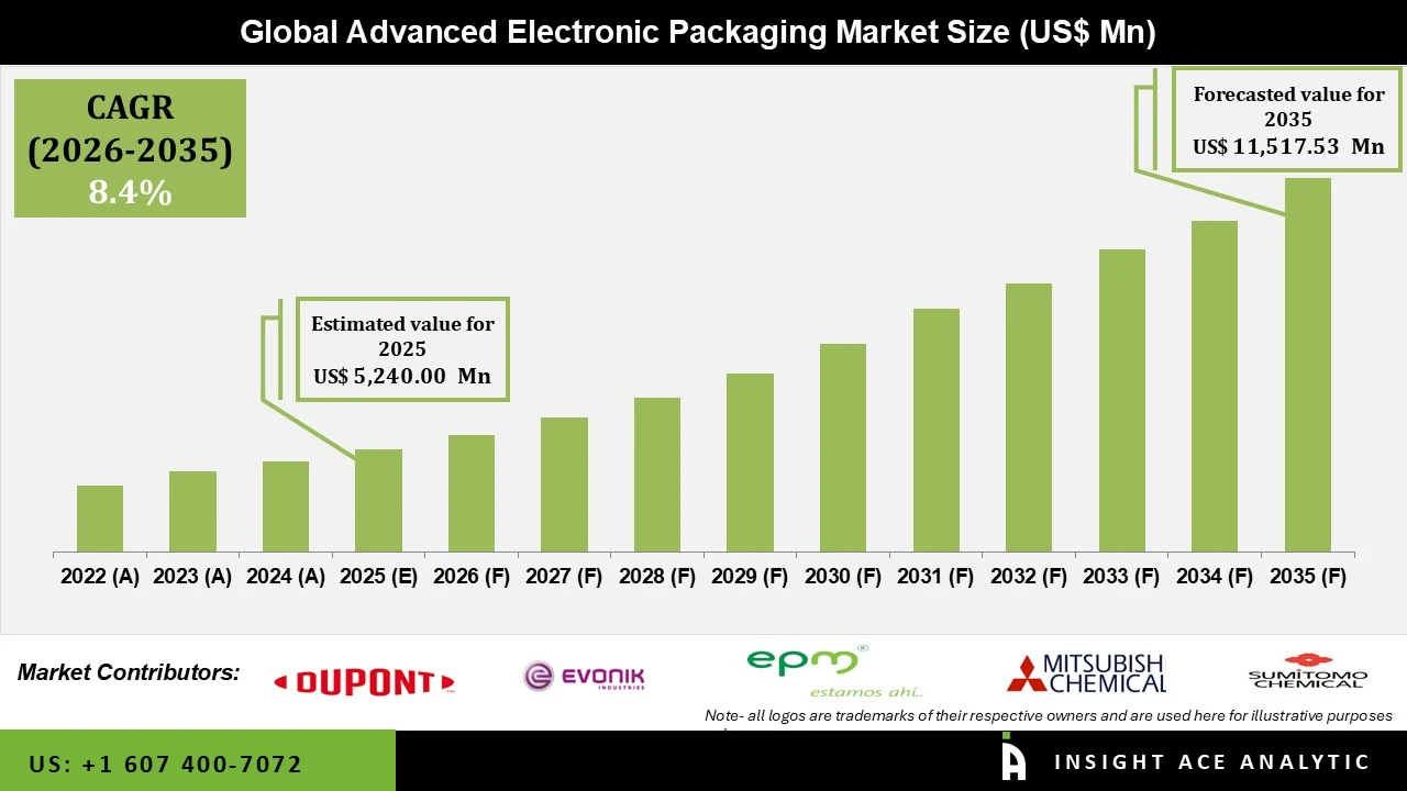
The advanced electronic packaging market encompasses materials, components, and packaging methods that protect electronic devices and enable them to operate more effectively and last longer. These packaging solutions connect semiconductor chips to printed circuit boards (PCBs), manage heat, reduce signal loss, and enable the development of smaller, faster, and more powerful electronics. Metal, plastic, and ceramic packages are commonly used in semiconductors, integrated circuits (ICs), PCBs, and other electronics. These technologies are important in many industries, including consumer electronics, automotive, telecommunications, industrial automation, aerospace, healthcare, and data centers, where there is a growing need for compact and high-performance systems.
The market is growing quickly because of advances in semiconductor technology and the need for smaller, lighter, and more powerful devices. As technologies like artificial intelligence (AI), 5G, electric vehicles (EVs), the Internet of Things (IoT), cloud computing, and high-performance computing become more common, manufacturers need packaging that manages heat better, transmits signals faster, and is more reliable. More people want smartphones, laptops, wearables, automotive electronics, industrial equipment, and networking devices, so companies are investing in new packaging materials and manufacturing methods to make devices work better while using less space and energy.
Manufacturers are creating new packaging materials, high-density interconnects, advanced substrates, and ceramic solutions that make products tougher and better at handling heat, while also supporting more complex chips. Technologies like 3D packaging, system-in-package (SiP), chiplet integration, and advanced bonding help companies deliver more computing power in smaller designs. More automation, precise manufacturing, and eco-friendly production are also improving quality and efficiency. Close teamwork among manufacturers, suppliers, electronics companies, and packaging experts is speeding up innovation and spreading advanced packaging across many industries. Even though the market is expected to grow, there are some challenges. Making advanced packaging solutions takes a lot of investment in research, special equipment, and high-quality materials. As chips get more complex, manufacturers have to solve problems with heat, signal quality, reliability, and costs. Issues like supply chain disruptions, changing material prices, and strict quality and environmental rules also make things harder.
Competitive Landscape
Which are the Leading Players in the Advanced Electronic Packaging Market?
• DuPont
• Evonik
• EPM
• Mitsubishi Chemical
• Sumitomo Chemical
• Mitsui High-tec
• Tanaka
• Shinko Electric Industries
• Panasonic
• Hitachi Chemical
• Kyocera Chemical
• Gore
• BASF
• Henkel
• AMETEK Electronic
• Toray
• Maruwa
• Leatec Fine Ceramics
• NCI
• Chaozhou Three-Circle
• Nippon Micrometal
• Toppan
• Dai Nippon Printing
• Possehl
• Ningbo Kangqiang
Market Dynamics
Driver
Growing Demand for High-Performance Electronics and Semiconductor Miniaturization
The advanced electronic packaging market is seeing steady growth as manufacturers focus on making electronic devices smaller, faster, and more energy-efficient. New technologies like artificial intelligence, 5G, electric vehicles, high-performance computing, cloud infrastructure, and the Internet of Things are increasing the need for advanced packaging that improves chip performance, heat management, and reliability. As chips become more complex, companies are putting money into new packaging materials and technologies that allow for more processing power, lower energy use, and smaller designs. Ongoing innovation in electronics and the growth of data centers and communication networks are also helping the market expand.
Restrain/Challenge
High Manufacturing Costs and Complex Packaging Processes
Even though the market is expected to grow, there are some challenges. Advanced electronic packaging needs special materials, precise manufacturing, and advanced equipment, which makes it costly to develop and produce. As chip designs get more complex, manufacturers have to solve problems like heat management, signal quality, reliability, and making sure new chips work with the latest technologies. Changes in raw material prices, supply chain issues, and strict quality and environmental rules also make operations more complicated. These challenges can slow down adoption, especially for companies with tight budgets.
Metal Packages Segment is Expected to Drive the Advanced Electronic Packaging Market
The Metal Packages segment is likely to make up a large part of the Advanced Electronic Packaging market because it offers strong thermal conductivity, mechanical strength, and protection for sensitive electronic parts in tough environments. These packages are common in power semiconductors, automotive electronics, aerospace, industrial equipment, and telecommunications, where good heat management and reliability matter most. As electronic devices get smaller and more powerful, the need for sturdy packaging that can handle high temperatures and harsh conditions is helping the metal packaging segment grow.
Semiconductor & IC Segment is Expected to Drive the Advanced Electronic Packaging Market
The Semiconductor & IC segment will likely lead the market since semiconductor chips are found in almost all modern electronic devices. More demand for smartphones, AI processors, data centers, 5G, automotive electronics, and industrial automation is pushing up production of advanced chips, which increases the need for high-performance packaging. Advanced electronic packaging improves electrical performance, heat management, miniaturization, and reliability, so it is a key part of making semiconductors. As chips become more complex, the Semiconductor & IC segment should stay the biggest area for advanced electronic packaging.
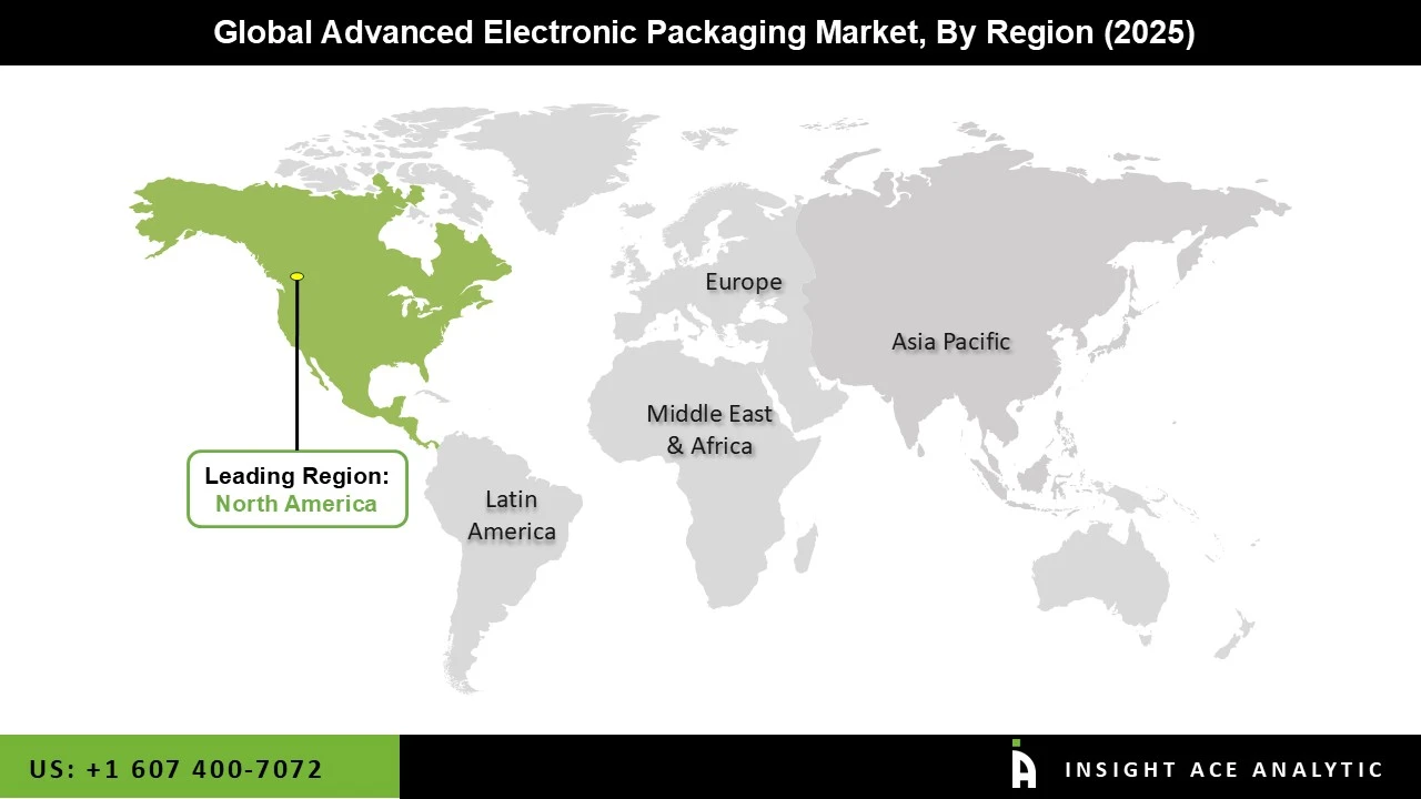
Why North America Leads the Advanced Electronic Packaging Market?
North America holds a leading position in the Advanced Electronic Packaging market due to its strong semiconductor ecosystem, advanced research capabilities, and continuous investment in next-generation electronics. The United States is home to many leading semiconductor manufacturers, technology companies, packaging solution providers, and research institutions that are driving innovation in advanced packaging technologies. Rising demand for AI computing, cloud infrastructure, defense electronics, automotive electronics, and high-performance computing continues to support market growth across the region. In addition, strong investments in semiconductor manufacturing, government support for domestic chip production, and ongoing advancements in packaging technologies are helping North America maintain its leadership in the global market.
Key Developments-
• In April 2025, DuPont (US) expanded its advanced electronic materials portfolio by introducing next-generation packaging materials designed to improve thermal management, electrical performance, and reliability for semiconductor and high-performance computing applications, supporting the growing demand for AI, 5G, and advanced chip packaging.
• In February 2025, Mitsubishi Chemical (Japan) strengthened its electronic materials business by advancing high-performance packaging materials for semiconductor and integrated circuit applications, with a focus on enhanced heat dissipation, miniaturisation, and improved durability for next-generation electronic devices.
Advanced Electronic Packaging Market Report Scope:
| Report Attribute | Specifications |
| Market size value in 2025 | USD 5,240.00 Mn |
| Revenue forecast in 2035 | USD 11,517.53 Mn |
| Growth Rate CAGR | CAGR of 8.4% from 2026 to 2035 |
| Quantitative Units | Representation of revenue in US$ Mn and CAGR from 2026 to 2035 |
| Historic Year | 2021 to 2025 |
| Forecast Year | 2026-2035 |
| Report Coverage | The forecast of revenue, the position of the company, the competitive market structure, growth prospects, and trends |
| Segments Covered | By Type, Application and By Region |
| Regional Scope | North America; Europe; Asia Pacific; Latin America; Middle East & Africa |
| Country Scope | U.S.; Canada; U.K.; Germany; China; India; Japan; Brazil; Mexico; The UK; France; Italy; Spain; China; Japan; India; South Korea; Southeast Asia; South Korea; Southeast Asia |
| Competitive Landscape | DuPont, Evonik, EPM, Mitsubishi Chemical, Sumitomo Chemical, Mitsui High-tec, Tanaka, Shinko Electric Industries, Panasonic, Hitachi Chemical, Kyocera Chemical, Gore, BASF, Henkel, AMETEK Electronic, Toray, Maruwa, Leatec Fine Ceramics, NCI, Chaozhou Three-Circle, Nippon Micrometal, Toppan, Dai Nippon Printing, Possehl, Ningbo Kangqiang |
| Customization Scope | Free customisation report with the procurement of the report, Modifications to the regional and segment scope. Geographic competitive landscape. |
| Pricing and Available Payment Methods | Explore pricing alternatives that are customized to your particular study requirements. |
Market Segmentation:
Advanced Electronic Packaging Market by Type -
• Metal Packages
• Plastic Packages
• Ceramic Packages
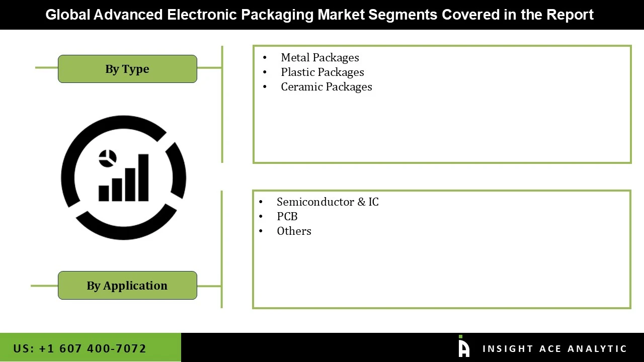
Advanced Electronic Packaging Market by Application-
• Semiconductor & IC
• PCB
• Others
Advanced Electronic Packaging Market by Region-
North America-
• The US
• Canada
Europe-
• Germany
• UK
• France
• Netherlands
• Switzerland
• Spain
• Italy
• Rest of Europe
Asia-Pacific-
• China
• Japan
• South Korea
• Australia
• India
• Rest of APAC
Latin America-
• Brazil
• Mexico
• Chile
• Rest of LatAm
Middle East & Africa-
• GCC
• South Africa
• Rest of MEA
Research Design and Approach
This study employed a multi-step, mixed-method research approach that integrates:
- Secondary research
- Primary research
- Data triangulation
- Hybrid top-down and bottom-up modelling
- Forecasting and scenario analysis
This approach ensures a balanced and validated understanding of both macro- and micro-level market factors influencing the market.
Secondary Research
Secondary research for this study involved the collection, review, and analysis of publicly available and paid data sources to build the initial fact base, understand historical market behaviour, identify data gaps, and refine the hypotheses for primary research.
Sources Consulted
Secondary data for the market study was gathered from multiple credible sources, including:
- Government databases, regulatory bodies, and public institutions
- International organizations (WHO, OECD, IMF, World Bank, etc.)
- Commercial and paid databases
- Industry associations, trade publications, and technical journals
- Company annual reports, investor presentations, press releases, and SEC filings
- Academic research papers, patents, and scientific literature
- Previous market research publications and syndicated reports
These sources were used to compile historical data, market volumes/prices, industry trends, technological developments, and competitive insights.
Primary Research
Primary research was conducted to validate secondary data, understand real-time market dynamics, capture price points and adoption trends, and verify the assumptions used in the market modelling.
Stakeholders Interviewed
Primary interviews for this study involved:
- Manufacturers and suppliers in the market value chain
- Distributors, channel partners, and integrators
- End-users / customers (e.g., hospitals, labs, enterprises, consumers, etc., depending on the market)
- Industry experts, technology specialists, consultants, and regulatory professionals
- Senior executives (CEOs, CTOs, VPs, Directors) and product managers
Interview Process
Interviews were conducted via:
- Structured and semi-structured questionnaires
- Telephonic and video interactions
- Email correspondences
- Expert consultation sessions
Primary insights were incorporated into demand modelling, pricing analysis, technology evaluation, and market share estimation.
Data Processing, Normalization, and Validation
All collected data were processed and normalized to ensure consistency and comparability across regions and time frames.
The data validation process included:
- Standardization of units (currency conversions, volume units, inflation adjustments)
- Cross-verification of data points across multiple secondary sources
- Normalization of inconsistent datasets
- Identification and resolution of data gaps
- Outlier detection and removal through algorithmic and manual checks
- Plausibility and coherence checks across segments and geographies
This ensured that the dataset used for modelling was clean, robust, and reliable.
Market Size Estimation and Data Triangulation
Bottom-Up Approach
The bottom-up approach involved aggregating segment-level data, such as:
- Company revenues
- Product-level sales
- Installed base/usage volumes
- Adoption and penetration rates
- Pricing analysis
This method was primarily used when detailed micro-level market data were available.
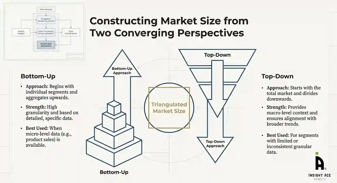
Top-Down Approach
The top-down approach used macro-level indicators:
- Parent market benchmarks
- Global/regional industry trends
- Economic indicators (GDP, demographics, spending patterns)
- Penetration and usage ratios
This approach was used for segments where granular data were limited or inconsistent.
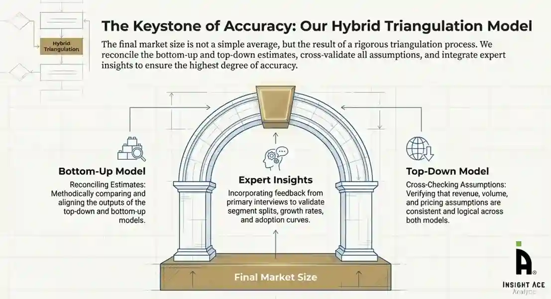
Hybrid Triangulation Approach
To ensure accuracy, a triangulated hybrid model was used. This included:
- Reconciling top-down and bottom-up estimates
- Cross-checking revenues, volumes, and pricing assumptions
- Incorporating expert insights to validate segment splits and adoption rates
This multi-angle validation yielded the final market size.
Forecasting Framework and Scenario Modelling
Market forecasts were developed using a combination of time-series modelling, adoption curve analysis, and driver-based forecasting tools.
Forecasting Methods
- Time-series modelling
- S-curve and diffusion models (for emerging technologies)
- Driver-based forecasting (GDP, disposable income, adoption rates, regulatory changes)
- Price elasticity models
- Market maturity and lifecycle-based projections
Scenario Analysis
Given inherent uncertainties, three scenarios were constructed:
- Base-Case Scenario: Expected trajectory under current conditions
- Optimistic Scenario: High adoption, favourable regulation, strong economic tailwinds
- Conservative Scenario: Slow adoption, regulatory delays, economic constraints
Sensitivity testing was conducted on key variables, including pricing, demand elasticity, and regional adoption.
Request Customization
Add countries, segments, company profiles, or extend forecast — free 10% customization with purchase.
Customize This Report →Enquire Before Buying
Speak with our analyst team about scope, methodology, pricing, or deliverable formats.
Enquire Now →Frequently Asked Questions
Advanced Electronic Packaging Market Size is valued at USD 5,240.00 Mn in 2025 and is predicted to reach USD 11,517.53 Mn by the year 2035
Advanced Electronic Packaging Market is expected to grow at a 8.4% CAGR during the forecast period for 2026 to 2035.
Advanced Electronic Packaging Market is segmented into By Type, Application and By Region
DuPont, Evonik, EPM, Mitsubishi Chemical, Sumitomo Chemical, Mitsui High-tec, Tanaka, Shinko Electric Industries, Panasonic, Hitachi Chemical, Kyocera Chemical, Gore, BASF, Henkel, AMETEK Electronic, Toray, Maruwa, Leatec Fine Ceramics, NCI, Chaozhou Three-Circle, Nippon Micrometal, Toppan, Dai Nippon Printing, Possehl, Ningbo Kangqiang
North America region is leading the Advanced Electronic Packaging Market.