Semiconductor Manufacturing Equipment Market Size, Trend, Revenue Report 2026 to 2035
What is Semiconductor Manufacturing Equipment Market Size?
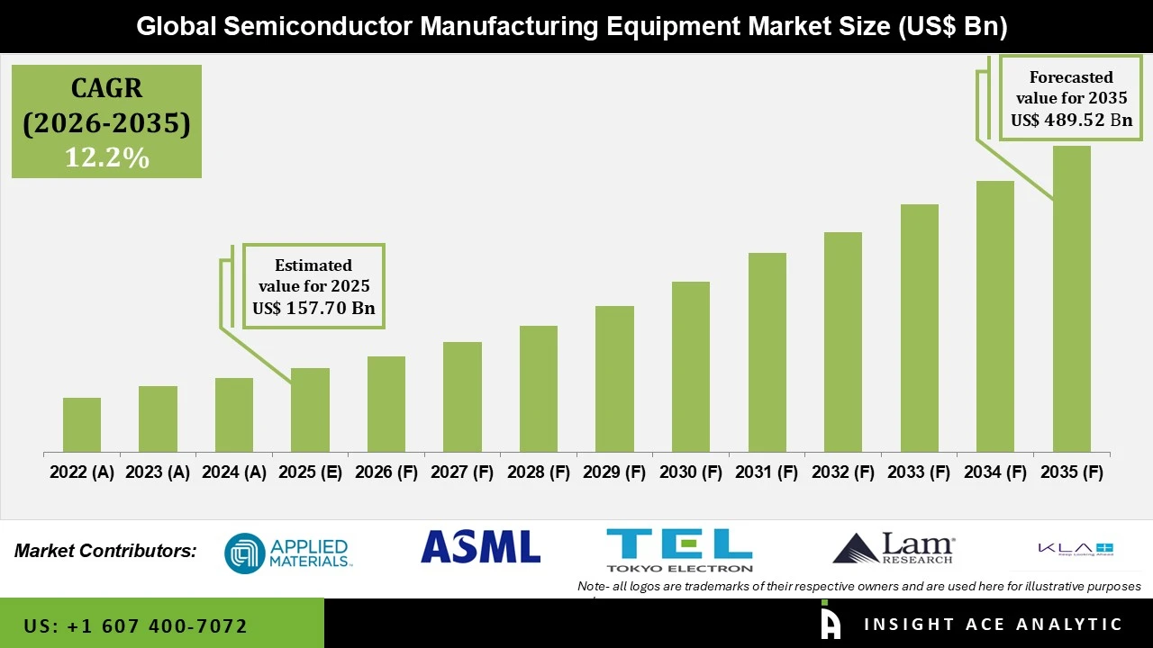
Semiconductor Manufacturing Equipment Market Size is valued at USD 157.70 Bn in 2025 and is predicted to reach USD 489.52 Bn by the year 2035 at a 12.2% CAGR during the forecast period for 2026 to 2035.
Semiconductor Manufacturing Equipment Market Size, Share & Trends Analysis By Front-end Equipment (Lithography (Photolithography (Deep Ultraviolet (DUV) Lithography, Extreme Ultraviolet (EUV) Lithography), Electron Beam Lithography, Ion Beam Lithography, Nanoimprint Lithography, Others), Wafer Surface Conditioning (Etching, Chemical Mechanical Planarization (CMP)), Wafer Cleaning, Deposition, Other Front-end Equipment), By Back-end Equipment, By Fab Facility Equipment, By Product Type, By Dimension, By Supply Chain Participant and Segment Forecasts, 2026 to 2035
Semiconductor manufacturing equipment refers to the specialized machinery, systems, and tools used in the fabrication, processing, assembly, packaging, and testing of semiconductor devices. These advanced equipment solutions enable the production of integrated circuits, memory chips, microprocessors, sensors, and other semiconductor components that serve as fundamental building blocks for modern electronic systems.
The growth of this semiconductor manufacturing equipment market is facilitated by rapidly emerging opportunities in the fields of artificial intelligence and high-performance computing. AI accelerators, GPUs, high bandwidth memory (HBM), and other processors demand advanced processing and packaging technologies. Therefore, as semiconductor architectures are becoming more sophisticated, manufacturers continue investing in advanced lithography, deposition, etching, inspection, metrology, and packaging equipment.
The increase in capital expenditures by new fabrication facilities is one more factor influencing the market. Many governments, in addition to semiconductor manufacturers in the United States, Europe, Japan, South Korea, Taiwan, China, and India are boosting the spending on developing local semiconductor ecosystems by increasing investments in fabrication facilities construction and expansion projects.
The growing adoption of advanced semiconductor technologies, such as smaller process nodes, 3D semiconductor architectures, advanced packaging, and high-performance computing solutions, is increasing the need for innovative manufacturing equipment.
Competitive Landscape
Which are the Leading Players in Semiconductor Manufacturing Equipment Market?
• Applied Materials, Inc.
• ASML Holding N.V.
• Lam Research Corporation
• Tokyo Electron Limited
• KLA Corporation
• SCREEN Holdings Co., Ltd.
• ASM International N.V.
• ASMPT Limited
• Teradyne, Inc.
• Advantest Corporation
• Kokusai Electric Corporation
• Hitachi High-Tech Corporation
• Onto Innovation Inc.
• DISCO Corporation
• Canon Machinery Inc.
• Nikon Corporation
• Kulicke & Soffa Industries, Inc.
• Axcelis Technologies, Inc.
• Veeco Instruments Inc.
• Tokyo Seimitsu Co., Ltd.
Market Dynamics
Driver
Increasing Demand for AI and High-Performance Computing Chips
Another very significant driver in favor of semiconductor fabrication equipment comes from the development of artificial intelligence and high-performance computing technology. Artificial intelligence accelerators and high-performance computing technology require state-of-the-art process nodes, advanced transistors, advanced packaging, and high bandwidth memory.
There is an increasing demand for advanced lithography, deposition, etching, inspection, and packaging equipment because of an increasing trend towards GPUs and custom-made AI accelerators. There is also an increasing need for production facilities in order to satisfy the demands of data centers.
High bandwidth memory is one of the components that make AI accelerators possible. High bandwidth memory is produced using advanced wafer processing techniques, stacking, bonding, packaging, and testing. All this results in additional need for fabrication equipment.
Restrain/Challenge
High Equipment Costs and Semiconductor Industry Cyclicality
One of the major obstacles in the semiconductor equipment manufacturing industry is the cost associated with sophisticated systems that enable manufacturing. Equipment for EUV lithography process, as well as deposition and etching tools, metrology machines, and advanced packaging tools require large capital investments.
Furthermore, the semiconductor industry is cyclic by nature. Demand for consumer electronics, memory prices, inventories, and semiconductor CapEx spending can be considered factors in semiconductor equipment orders. During the periods of weak demand for chips, suppliers could postpone their plans for building new fabs or purchasing equipment.
Also, there are export restrictions that represent an issue for manufacturers and suppliers of semiconductor equipment. Today, more and more companies that produce semiconductor equipment operate in quite difficult regulation environment, especially for advanced manufacturing solutions.
lithography equipment Segment is Expected to Drive the Semiconductor Manufacturing Equipment Market
Front-end equipment remains the leading segment in the semiconductor manufacturing equipment market, accounting for the majority of revenue due to its critical role in wafer fabrication processes such as lithography, deposition, etching, cleaning, and metrology. Within this category, lithography equipment particularly extreme ultraviolet (EUV) systems dominates because it enables the precise patterning required for advanced nodes (5 nm, 3 nm, and beyond). High capital intensity, continuous technology upgrades driven by AI, high-performance computing, and 5G demand, and the need for finer feature sizes keep front-end tools as the primary growth and investment focus for foundries and IDMs.
Assembly & Packaging is Gaining Importance
In the back-end segment, testing equipment currently holds the largest share as every device must undergo rigorous functional and reliability checks before shipment, while assembly & packaging is the fastest-growing subsegment. The shift toward advanced packaging technologies—including 2.5D/3D stacking, hybrid bonding, fan-out wafer-level packaging, and chiplet architectures—is driving strong demand for precision bonding, dicing, and packaging tools. Among end users, foundries lead in market share due to their large-scale capacity expansions, while OSAT companies are expanding most rapidly as outsourcing of advanced packaging and testing continues to rise.
Why Asia Pacific Led the Semiconductor Manufacturing Equipment Market?
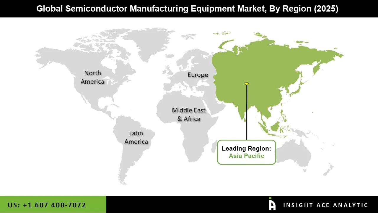
Asia Pacific continues to be the predominant region in terms of semiconductor manufacturing equipment due to the presence of extensive semiconductor manufacturing capabilities. Taiwan, South Korea, China, and Japan combined constitute a significant share of global semiconductor manufacturing capabilities and demand for equipment.
The significance of Taiwan is due to the presence of extensive foundry capabilities and investments in semiconductor manufacturing at leading edge technology nodes. The significance of South Korea arises out of being a memory producing region including DRAM and HBM and Japan due to its semiconductor materials and equipment capabilities.
China too emerges as a major equipment buyer in view of the investments in domestic semiconductor manufacturing. While some technologies become off-limits due to export restrictions, the investments continue in terms of mature node capabilities and domestic equipment.
North America would experience significant growth as a region as domestic semiconductor manufacturing picks up in the United States in line with CHIPS and Science Act. Investments in Fab facilities by major semiconductor manufacturing companies would drive wafer-fabrication, packaging, inspection, and testing equipment.
Similarly, Europe would also see increased investments in semiconductors including the development of European Chips Act. New Fabs under development would result in an addition to the demand for semiconductor manufacturing equipment.
Key Development:
• In January 2026, Tokyo Electron reported an increased expansion of its semiconductor production equipment product portfolio, with advanced packaging gaining importance along with traditional technologies of wafer processing. Advanced packaging and traditional wafer processing equipment such as coater/developer, plasma etch, deposition, cleaning, probing, and bonding are mentioned among the strongest competencies of the company.
Semiconductor Manufacturing Equipment Market Report Scope:
| Report Attribute | Specifications |
| Market size value in 2025 | USD 157.70 Bn |
| Revenue forecast in 2035 | USD 489.52 Bn |
| Growth Rate CAGR | CAGR of 12.2% from 2026 to 2035 |
| Quantitative Units | Representation of revenue in US$ Bn and CAGR from 2026 to 2035 |
| Historic Year | 2022 to 2025 |
| Forecast Year | 2026-2035 |
| Report Coverage | The forecast of revenue, the position of the company, the competitive market structure, growth prospects, and trends |
| Segments Covered | Front-End Equipment, Back-end Equipment, Product Type, Supply Chain Partcipant, Fab Facility Equipment, Dimension and By Region |
| Regional Scope | North America; Europe; Asia Pacific; Latin America; Middle East & Africa |
| Country Scope | U.S.; Canada; U.K.; Germany; China; India; Japan; Brazil; Mexico; France; Italy; Spain; South Korea; Southeast Asia |
| Competitive Landscape | Applied Materials Inc., ASML Holding N.V., Lam Research Corporation, Tokyo Electron Limited, KLA Corporation, SCREEN Holdings Co. Ltd., ASM International N.V., ASMPT Limited, Teradyne Inc., Advantest Corporation, Kokusai Electric Corporation, Hitachi High-Tech Corporation, Onto Innovation Inc., DISCO Corporation, Canon Machinery Inc., Nikon Corporation, Kulicke & Soffa Industries Inc., Axcelis Technologies Inc., Veeco Instruments Inc., and Tokyo Seimitsu Co. Ltd. |
| Customization Scope | Free customization report with the procurement of the report, Modifications to the regional and segment scope. Geographic competitive landscape. |
| Pricing and Available Payment Methods | Explore pricing alternatives that are customized to your particular study requirements. |
Market Segmentation:
Semiconductor Manufacturing Equipment Market By Front-end Equipment
• Lithography
o Photolithography
Deep Ultraviolet (DUV) Lithography
Extreme Ultraviolet (EUV) Lithography
o Electron Beam Lithography
o Ion Beam Lithography
o Nanoimprint Lithography
o Others
• Wafer Surface Conditioning
o Etching
o Chemical Mechanical Planarization (CMP)
• Wafer Cleaning
• Deposition
• Other Front-end Equipment
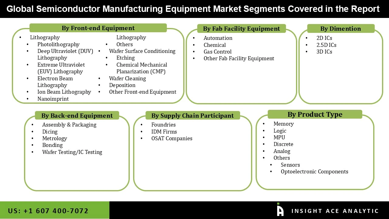
Semiconductor Manufacturing Equipment Market By Back-end Equipment
• Assembly & Packaging
• Dicing
• Metrology
• Bonding
• Wafer Testing/IC Testing
Semiconductor Manufacturing Equipment Market By Fab Facility Equipment
• Automation
• Chemical
• Gas Control
• Other Fab Facility Equipment
Semiconductor Manufacturing Equipment Market By Product Type
• Memory
• Logic
• MPU
• Discrete
• Analog
• Others
o Sensors
o Optoelectronic Components
Semiconductor Manufacturing Equipment Market By Dimension
• 2D ICs
• 2.5D ICs
• 3D ICs
Semiconductor Manufacturing Equipment Market By Supply Chain Participant
• Foundries
• IDM Firms
• OSAT Companies
Semiconductor Manufacturing Equipment Market By Region-
North America-
• The US
• Canada
Europe-
• Germany
• The UK
• France
• Italy
• Spain
• Rest of Europe
Asia-Pacific-
• China
• Japan
• India
• South Korea
• South East Asia
• Rest of Asia Pacific
Latin America-
• Brazil
• Argentina
• Mexico
• Rest of Latin America
Middle East & Africa-
• GCC Countries
• South Africa
• Rest of Middle East and Africa
Research Design and Approach
This study employed a multi-step, mixed-method research approach that integrates:
- Secondary research
- Primary research
- Data triangulation
- Hybrid top-down and bottom-up modelling
- Forecasting and scenario analysis
This approach ensures a balanced and validated understanding of both macro- and micro-level market factors influencing the market.
Secondary Research
Secondary research for this study involved the collection, review, and analysis of publicly available and paid data sources to build the initial fact base, understand historical market behaviour, identify data gaps, and refine the hypotheses for primary research.
Sources Consulted
Secondary data for the market study was gathered from multiple credible sources, including:
- Government databases, regulatory bodies, and public institutions
- International organizations (WHO, OECD, IMF, World Bank, etc.)
- Commercial and paid databases
- Industry associations, trade publications, and technical journals
- Company annual reports, investor presentations, press releases, and SEC filings
- Academic research papers, patents, and scientific literature
- Previous market research publications and syndicated reports
These sources were used to compile historical data, market volumes/prices, industry trends, technological developments, and competitive insights.
Primary Research
Primary research was conducted to validate secondary data, understand real-time market dynamics, capture price points and adoption trends, and verify the assumptions used in the market modelling.
Stakeholders Interviewed
Primary interviews for this study involved:
- Manufacturers and suppliers in the market value chain
- Distributors, channel partners, and integrators
- End-users / customers (e.g., hospitals, labs, enterprises, consumers, etc., depending on the market)
- Industry experts, technology specialists, consultants, and regulatory professionals
- Senior executives (CEOs, CTOs, VPs, Directors) and product managers
Interview Process
Interviews were conducted via:
- Structured and semi-structured questionnaires
- Telephonic and video interactions
- Email correspondences
- Expert consultation sessions
Primary insights were incorporated into demand modelling, pricing analysis, technology evaluation, and market share estimation.
Data Processing, Normalization, and Validation
All collected data were processed and normalized to ensure consistency and comparability across regions and time frames.
The data validation process included:
- Standardization of units (currency conversions, volume units, inflation adjustments)
- Cross-verification of data points across multiple secondary sources
- Normalization of inconsistent datasets
- Identification and resolution of data gaps
- Outlier detection and removal through algorithmic and manual checks
- Plausibility and coherence checks across segments and geographies
This ensured that the dataset used for modelling was clean, robust, and reliable.
Market Size Estimation and Data Triangulation
Bottom-Up Approach
The bottom-up approach involved aggregating segment-level data, such as:
- Company revenues
- Product-level sales
- Installed base/usage volumes
- Adoption and penetration rates
- Pricing analysis
This method was primarily used when detailed micro-level market data were available.
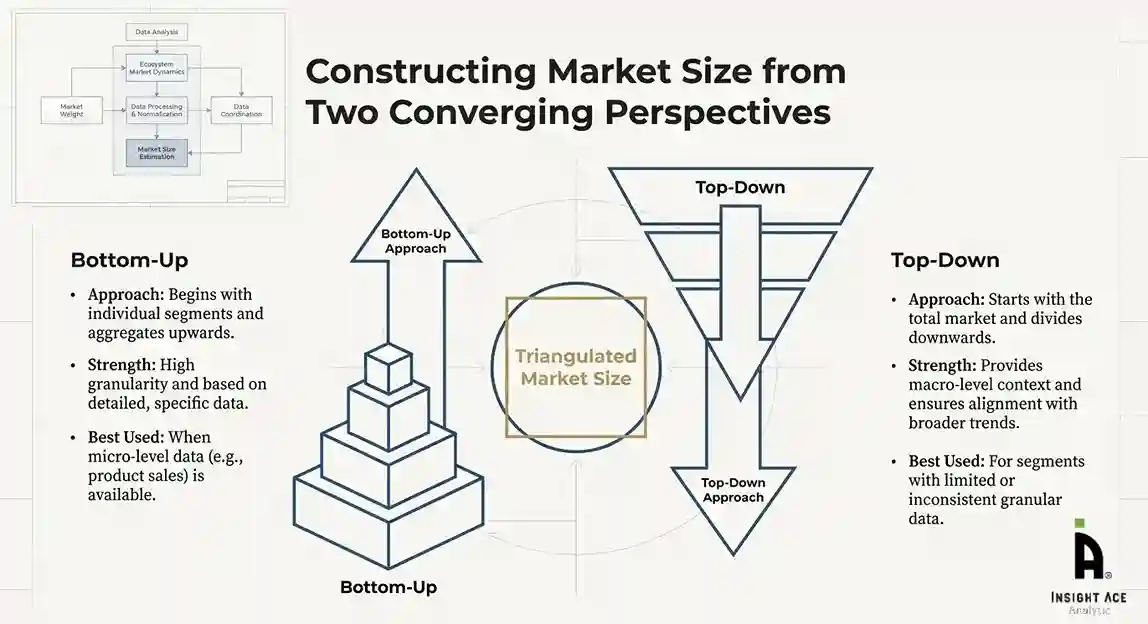
Top-Down Approach
The top-down approach used macro-level indicators:
- Parent market benchmarks
- Global/regional industry trends
- Economic indicators (GDP, demographics, spending patterns)
- Penetration and usage ratios
This approach was used for segments where granular data were limited or inconsistent.
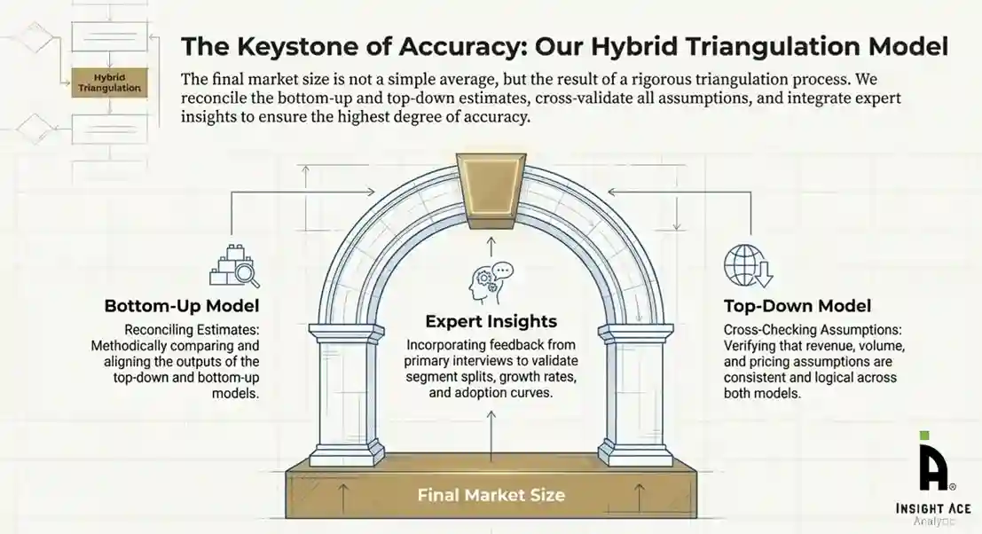
Hybrid Triangulation Approach
To ensure accuracy, a triangulated hybrid model was used. This included:
- Reconciling top-down and bottom-up estimates
- Cross-checking revenues, volumes, and pricing assumptions
- Incorporating expert insights to validate segment splits and adoption rates
This multi-angle validation yielded the final market size.
Forecasting Framework and Scenario Modelling
Market forecasts were developed using a combination of time-series modelling, adoption curve analysis, and driver-based forecasting tools.
Forecasting Methods
- Time-series modelling
- S-curve and diffusion models (for emerging technologies)
- Driver-based forecasting (GDP, disposable income, adoption rates, regulatory changes)
- Price elasticity models
- Market maturity and lifecycle-based projections
Scenario Analysis
Given inherent uncertainties, three scenarios were constructed:
- Base-Case Scenario: Expected trajectory under current conditions
- Optimistic Scenario: High adoption, favourable regulation, strong economic tailwinds
- Conservative Scenario: Slow adoption, regulatory delays, economic constraints
Sensitivity testing was conducted on key variables, including pricing, demand elasticity, and regional adoption.
Request Customization
Add countries, segments, company profiles, or extend forecast — free 10% customization with purchase.
Customize This Report →Enquire Before Buying
Speak with our analyst team about scope, methodology, pricing, or deliverable formats.
Enquire Now →Frequently Asked Questions
Semiconductor Manufacturing Equipment Market Size is valued at USD 157.70 Bn in 2025 and is predicted to reach USD 489.52 Bn by the year 2035
Semiconductor Manufacturing Equipment Market is expected to grow at a 12.2% CAGR during the forecast period for 2026 to 2035.
Applied Materials Inc., ASML Holding N.V., Lam Research Corporation, Tokyo Electron Limited, KLA Corporation, SCREEN Holdings Co. Ltd., ASM International N.V., ASMPT Limited, Teradyne Inc., Advantest Corporation, Kokusai Electric Corporation, Hitachi High-Tech Corporation, Onto Innovation Inc., DISCO Corporation, Canon Machinery Inc., Nikon Corporation, Kulicke & Soffa Industries Inc., Axcelis Technologies Inc., Veeco Instruments Inc., and Tokyo Seimitsu Co. Ltd.
Semiconductor Manufacturing Equipment Market is segmented into Front-End Equipment, Back-end Equipment, Product Type, Supply Chain Partcipant, Fab Facility Equipment, Dimension and By Region
Asia Pacific region is leading the Semiconductor Manufacturing Equipment Market.