GaN Substrate Market Size, Share, Trend Report 2026 to 2035
What is GaN Substrate Market Size?
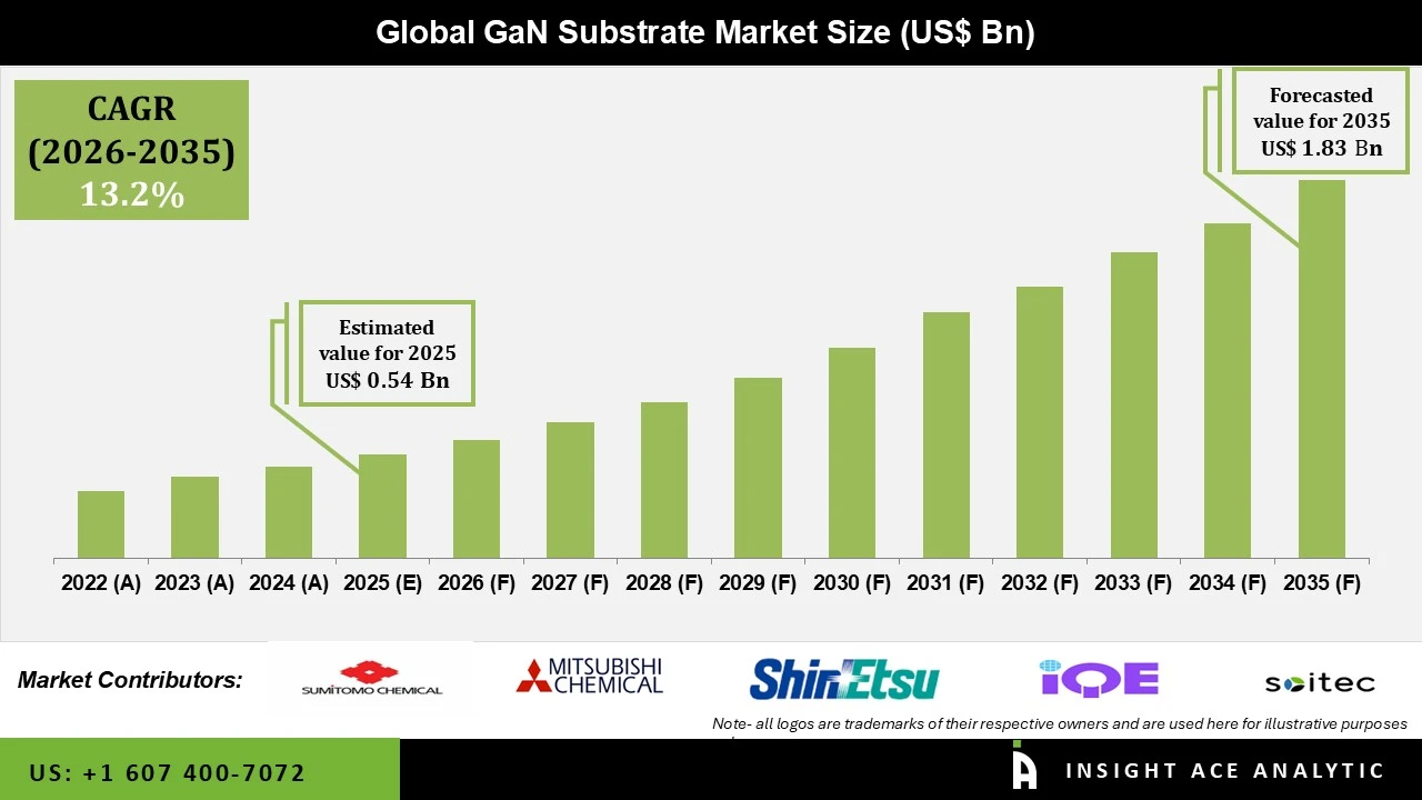
GaN Substrate Market Size is valued at USD 0.54 Bn in 2025 and is predicted to reach USD 1.83 Bn by the year 2035 at a 13.2% CAGR during the forecast period for 2026 to 2035.
GaN Substrate Market Size, Share & Trends Analysis By Substrate Type (GaN-on-SiC, GaN-on-Si, GaN-on-Sapphire, Bulk GaN, and Others), Wafer Size (2-inch, 4-inch, 6-inch, and 6-inch & Above), Application (RF Devices, Power Electronics, Optoelectronics, Laser Diodes, and Automotive Electronics), End-use Industry (Consumer Electronics, Telecommunications, Automotive, Aerospace & Defense, Healthcare, Energy & Power, and Others), and Segment Forecasts, 2026 to 2035
GaN Substrates are semiconductor substrates that serve as a base to grow GaN layers and produce power, RF, and optoelectronics. With its high strength of breakdown voltage, high switching speed, and high thermal characteristics, GaN helps manufacturers create smaller and more effective electronic systems. The market of GaN Substrates is growing with an increase in demand for power-efficient electronic devices, 5G and future 6G networks, electric cars, fast chargers, power electronics, etc.
Moreover, the trend towards high-quality bulk GaN substrates and specially engineered substrates for eliminating defects and increasing the performance of devices is observed on the market. The substrate quality is still relevant since crystal defects, uniformity of wafers, their surface characteristics and thermal behavior influence epitaxy process and affect device yield. Thus, companies make investments into development of larger wafer diameters, new methods of crystal growth, and substrate structures suitable for power and high frequency applications.
Other relevant trends on the market include larger wafers and technologies related to specific applications. Six-inch wafers and above allow getting higher volume of production and reducing costs of substrates per each device. At the same time, the GaN on SiC is necessary for high frequency RF and high power electronic devices while bulk GaN is required for low defect density and high quality material.
Competitive Landscape
Which are the Leading Players in GaN Substrate Market?
• Sumitomo Chemical Co., Ltd.
• Sumitomo Electric Industries, Ltd.
• Mitsubishi Chemical Corporation
• Shin-Etsu Chemical Co., Ltd.
• Soitec SA
• IQE plc
• Wolfspeed, Inc.
• Kyma Technologies, Inc.
• Coherent Corp.
• Qorvo, Inc.
• NXP Semiconductors N.V.
• Infineon Technologies AG
• MACOM Technology Solutions Holdings, Inc.
• TDK Corporation
• SK Siltron Co., Ltd.
• Saint-Gobain
• Kyocera Corporation
• Toshiba Corporation
• Fujitsu Limited
• NTT Advanced Technology Corporation
Market Dynamics
Driver
Growing Demand for High-Efficiency Power and RF Devices
Increasing application of GaN devices in power electronics and RF components is amongst the key driving forces that are contributing to the growth of the GaN Substrate Market. GaN semiconductor devices have capability to handle higher switching frequency levels, power density, and lower losses compared to traditional Si semiconductor devices in compatible applications. There has been an increase in the demand for the product in applications ranging from fast charger technology, data center power supplies, telecom base stations, auto electronics, renewable energy, and space & defense sector.
Restrain/Challenge
High Manufacturing Cost and Crystal-Growth Complexity
Production of GaN substrates is more challenging and expensive compared to the production of traditional silicon substrates. GaN crystal growth and control of defects during GaN wafers processing, including polishing, requires special equipment and special knowledge. Production of large diameter bulk GaN substrates poses technical challenges too. This could lead to increasing the cost of substrates or slow down their adoption when there are alternative cheaper materials like GaN on Si.
Bulk GaN Segment is Expected to Drive the GaN Substrate Market
The Bulk GaN segment continues to be an important one owing to the high crystal GaN base available here with low lattice mismatch in GaN devices. The use of these segments is fueled by the need for devices with high-quality, high thermal properties, and reliable devices especially those with power electronics, RF devices, and optoelectronic devices.
GaN on SiC is an important technology as silicon carbide is known to have excellent thermal properties with support in high-frequency and high-power RF devices.
6-inch and Above Wafer Segment is Expected to Gain Importance
Increasing wafer diameters play an essential role due to higher productivity and reduced cost per unit required by the producers. Larger diameter may facilitate fabrication process, but greater level of control on the crystal growth and wafer quality is necessary. Thus, development of large-size substrates is critical competitive field for suppliers.
Wafers with smaller diameters such as 2-inch still have application for research, prototyping, laser diodes, and special purpose devices. This kind of substrate offers a cheaper way to enter in development process, whereas 4-inch wafers are used for standard processes.
Why Asia Pacific Led the GaN Substrate Market?
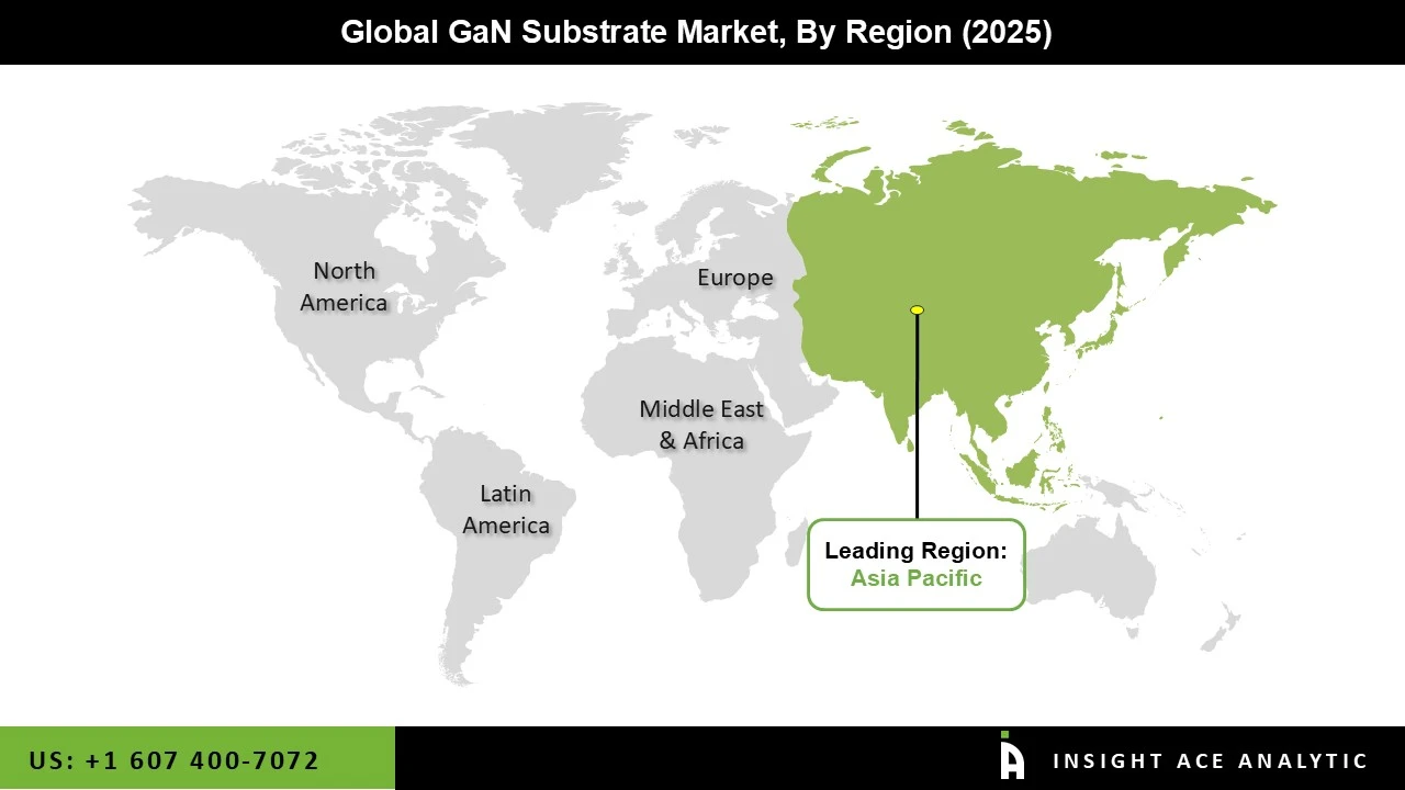
In the GaN Substrate Market in 2025, Asia Pacific emerged as the market leader. It benefits from a highly developed manufacturing industry of semiconductor, electronics, telecommunication, automotive and optoelectronics components. Compound semiconductor manufacturing is available in Japan, China, South Korea and Taiwan, and investment in advanced semiconductor power devices is expected to increase regional demand.
However, Japan is one of the most valuable markets for the industry because many leading players are present on it. These include Sumitomo Chemical, Sumitomo Electric, Mitsubishi Chemical, Shin-Etsu and others, which have extensive involvement in advanced semiconductor materials. Research into bulk GaN crystal growth and power-device technologies is conducted in Japan. In addition, in recent years, both China and South Korea have increased investment in building national supply chains for semiconductors, and Taiwan is an essential player because of its advanced semiconductor manufacturing ecosystem.
India becomes a growing opportunity due to electronics manufacturing, electric vehicle development, telecommunications networks, energy generation and semiconductor manufacturing initiatives. In the context of increasing importance of energy efficient power electronics, it can help drive demand for GaN substrates and epitaxial materials in the future.
North America is still an important location for the development of RF technology, aerospace and defense, data center, automotive electronics and power semiconductors segments. There are already existing GaN device and substrate companies and solid research activity around the area of wide bandgap semiconductors.
GaN Substrate Market Report Scope:
| Report Attribute | Specifications |
| Market size value in 2025 | USD 0.54 Bn |
| Revenue forecast in 2035 | USD 1.83 Bn |
| Growth Rate CAGR | CAGR of 13.2% from 2026 to 2035 |
| Quantitative Units | Representation of revenue in US$ Bn and CAGR from 2026 to 2035 |
| Historic Year | 2022 to 2025 |
| Forecast Year | 2026-2035 |
| Report Coverage | The forecast of revenue, the position of the company, the competitive market structure, growth prospects, and trends |
| Segments Covered | Substrate Type, Wafer Size, Application, End-use Industry, and By Region |
| Regional Scope | North America; Europe; Asia Pacific; Latin America; Middle East & Africa |
| Country Scope | U.S.; Canada; U.K.; Germany; China; India; Japan; Brazil; Mexico; The UK; France; Italy; Spain; China; Japan; India; South Korea; Southeast Asia; South Korea; Southeast Asia |
| Competitive Landscape | Sumitomo Chemical, Sumitomo Electric, Mitsubishi Chemical, Shin-Etsu Chemical, Soitec, IQE, Wolfspeed, Kyma Technologies, Coherent, Qorvo, NXP Semiconductors, Infineon Technologies, MACOM, TDK, SK Siltron, Saint-Gobain, Kyocera, Toshiba, Fujitsu, and NTT Advanced Technology. |
| Customization Scope | Free customization report with the procurement of the report, Modifications to the regional and segment scope. Geographic competitive landscape. |
| Pricing and Available Payment Methods | Explore pricing alternatives that are customized to your particular study requirements. |
Market Segmentation:
GaN Substrate Market by Substrate Type -
• GaN-on-SiC
• GaN-on-Si
• GaN-on-Sapphire
• Bulk GaN
• Others
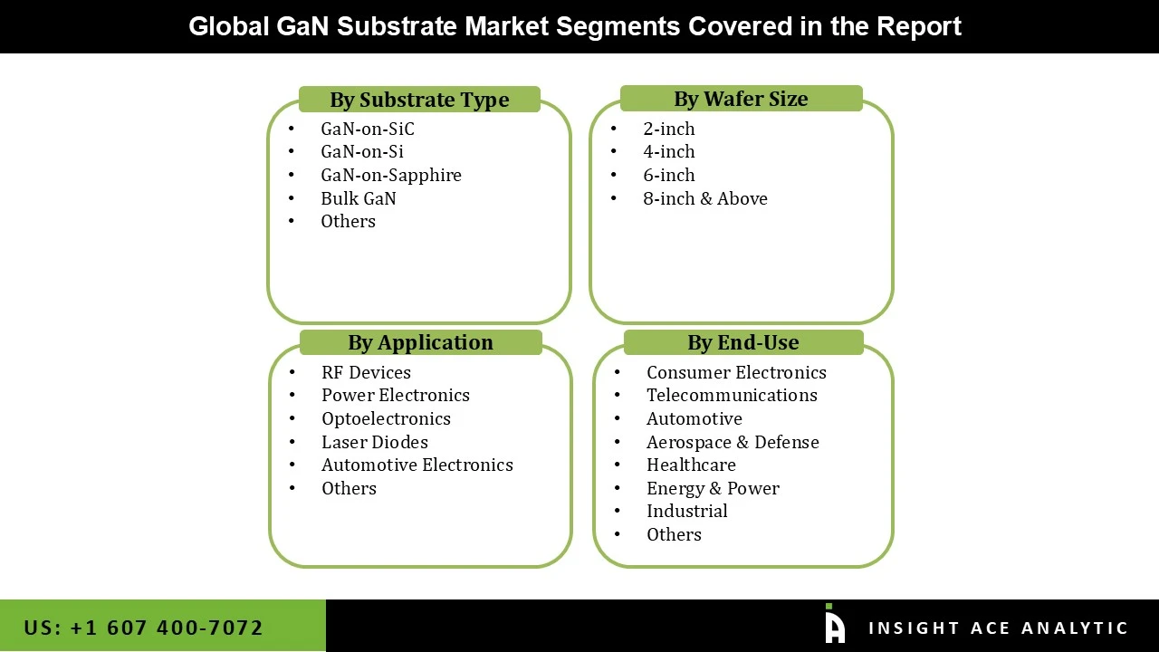
GaN Substrate Market by Wafer Size -
• 2-inch
• 4-inch
• 6-inch
• 6-inch & Above
GaN Substrate Market Application -
• RF Devices
• Power Electronics
• Optoelectronics
• Laser Diodes
• Automotive Electronics
GaN Substrate Market End-user Industry -
• Consumer Electronics
• Telecommunications
• Automotive
• Aerospace & Defense
• Healthcare
• Energy & Power
• Industrial
• Others
GaN Substrate Market By Region-
North America-
• The US
• Canada
Europe-
• Germany
• The UK
• France
• Italy
• Spain
• Rest of Europe
Asia-Pacific-
• China
• Japan
• India
• South Korea
• South East Asia
• Rest of Asia Pacific
Latin America-
• Brazil
• Argentina
• Mexico
• Rest of Latin America
Middle East & Africa-
• GCC Countries
• South Africa
• Rest of Middle East and Africa
Research Design and Approach
This study employed a multi-step, mixed-method research approach that integrates:
- Secondary research
- Primary research
- Data triangulation
- Hybrid top-down and bottom-up modelling
- Forecasting and scenario analysis
This approach ensures a balanced and validated understanding of both macro- and micro-level market factors influencing the market.
Secondary Research
Secondary research for this study involved the collection, review, and analysis of publicly available and paid data sources to build the initial fact base, understand historical market behaviour, identify data gaps, and refine the hypotheses for primary research.
Sources Consulted
Secondary data for the market study was gathered from multiple credible sources, including:
- Government databases, regulatory bodies, and public institutions
- International organizations (WHO, OECD, IMF, World Bank, etc.)
- Commercial and paid databases
- Industry associations, trade publications, and technical journals
- Company annual reports, investor presentations, press releases, and SEC filings
- Academic research papers, patents, and scientific literature
- Previous market research publications and syndicated reports
These sources were used to compile historical data, market volumes/prices, industry trends, technological developments, and competitive insights.
Primary Research
Primary research was conducted to validate secondary data, understand real-time market dynamics, capture price points and adoption trends, and verify the assumptions used in the market modelling.
Stakeholders Interviewed
Primary interviews for this study involved:
- Manufacturers and suppliers in the market value chain
- Distributors, channel partners, and integrators
- End-users / customers (e.g., hospitals, labs, enterprises, consumers, etc., depending on the market)
- Industry experts, technology specialists, consultants, and regulatory professionals
- Senior executives (CEOs, CTOs, VPs, Directors) and product managers
Interview Process
Interviews were conducted via:
- Structured and semi-structured questionnaires
- Telephonic and video interactions
- Email correspondences
- Expert consultation sessions
Primary insights were incorporated into demand modelling, pricing analysis, technology evaluation, and market share estimation.
Data Processing, Normalization, and Validation
All collected data were processed and normalized to ensure consistency and comparability across regions and time frames.
The data validation process included:
- Standardization of units (currency conversions, volume units, inflation adjustments)
- Cross-verification of data points across multiple secondary sources
- Normalization of inconsistent datasets
- Identification and resolution of data gaps
- Outlier detection and removal through algorithmic and manual checks
- Plausibility and coherence checks across segments and geographies
This ensured that the dataset used for modelling was clean, robust, and reliable.
Market Size Estimation and Data Triangulation
Bottom-Up Approach
The bottom-up approach involved aggregating segment-level data, such as:
- Company revenues
- Product-level sales
- Installed base/usage volumes
- Adoption and penetration rates
- Pricing analysis
This method was primarily used when detailed micro-level market data were available.
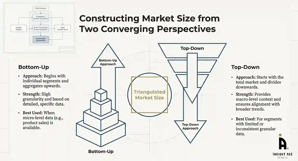
Top-Down Approach
The top-down approach used macro-level indicators:
- Parent market benchmarks
- Global/regional industry trends
- Economic indicators (GDP, demographics, spending patterns)
- Penetration and usage ratios
This approach was used for segments where granular data were limited or inconsistent.
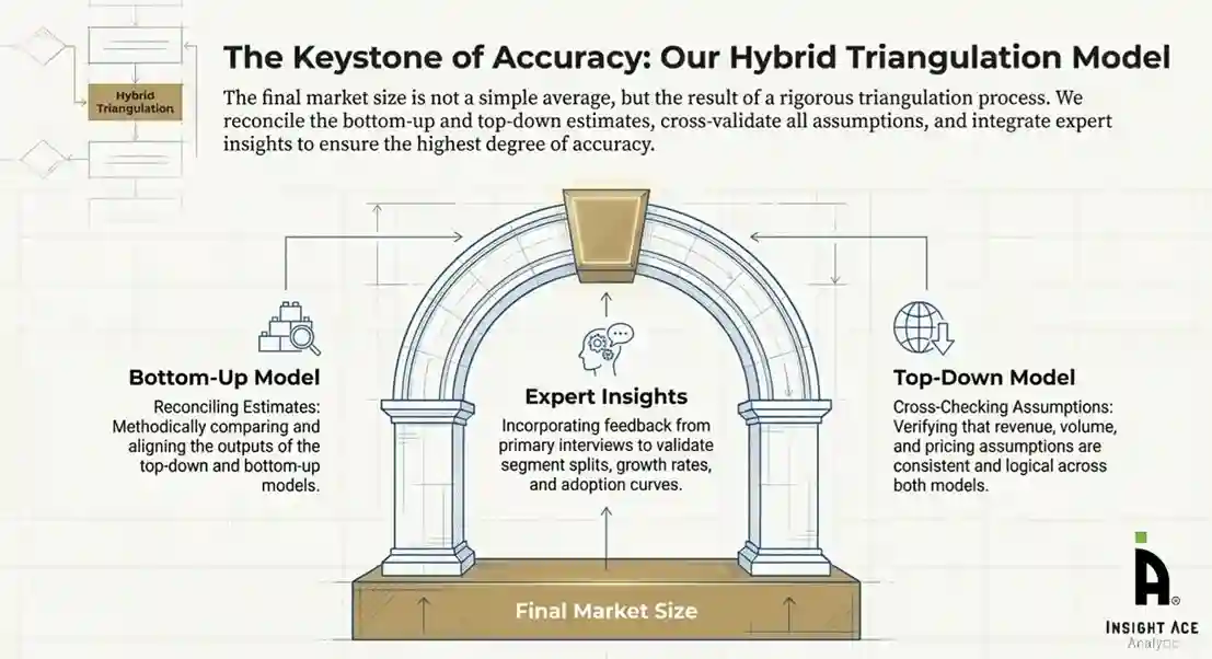
Hybrid Triangulation Approach
To ensure accuracy, a triangulated hybrid model was used. This included:
- Reconciling top-down and bottom-up estimates
- Cross-checking revenues, volumes, and pricing assumptions
- Incorporating expert insights to validate segment splits and adoption rates
This multi-angle validation yielded the final market size.
Forecasting Framework and Scenario Modelling
Market forecasts were developed using a combination of time-series modelling, adoption curve analysis, and driver-based forecasting tools.
Forecasting Methods
- Time-series modelling
- S-curve and diffusion models (for emerging technologies)
- Driver-based forecasting (GDP, disposable income, adoption rates, regulatory changes)
- Price elasticity models
- Market maturity and lifecycle-based projections
Scenario Analysis
Given inherent uncertainties, three scenarios were constructed:
- Base-Case Scenario: Expected trajectory under current conditions
- Optimistic Scenario: High adoption, favourable regulation, strong economic tailwinds
- Conservative Scenario: Slow adoption, regulatory delays, economic constraints
Sensitivity testing was conducted on key variables, including pricing, demand elasticity, and regional adoption.
Request Customization
Add countries, segments, company profiles, or extend forecast — free 10% customization with purchase.
Customize This Report →Enquire Before Buying
Speak with our analyst team about scope, methodology, pricing, or deliverable formats.
Enquire Now →Frequently Asked Questions
GaN Substrate Market Size is valued at USD 0.54 Bn in 2025 and is predicted to reach USD 1.83 Bn by the year 2035
GaN Substrate Market is expected to grow at a 13.2% CAGR during the forecast period for 2026 to 2035.
Sumitomo Chemical, Sumitomo Electric, Mitsubishi Chemical, Shin-Etsu Chemical, Soitec, IQE, Wolfspeed, Kyma Technologies, Coherent, Qorvo, NXP Semiconductors, Infineon Technologies, MACOM, TDK, SK Siltron, Saint-Gobain, Kyocera, Toshiba, Fujitsu, and NTT Advanced Technology.
GaN Substrate Market is segmented into Substrate Type, Wafer Size, Application, End-use Industry, and By Region
Asia Pacific region is leading the GaN Substrate Market.