Photolithography Optimization AI Market Size, Share, Trend, Revenue Report 2026 to 2035
What is Photolithography Optimization AI Market Size?
Photolithography Optimization AI Market Size is valued at USD 2.15 Bn in 2025 and is predicted to reach USD 11.16 Bn by the year 2035 at a 18.0% CAGR during the forecast period for 2026 to 2035.
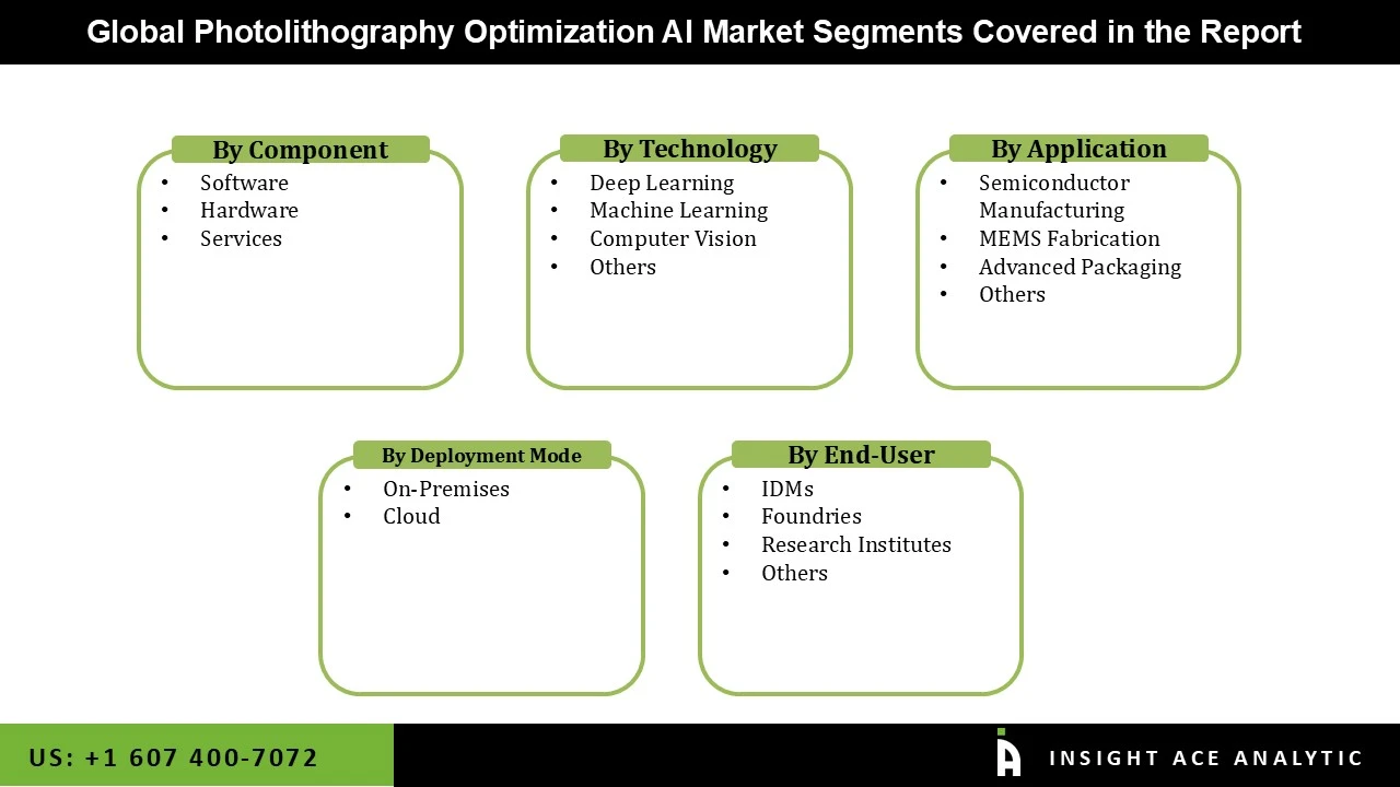
Photolithography Optimization AI Market Size, Share & Trends Analysis by Component (Software, Hardware, Services), by Technology (Deep Learning, Machine Learning, Computer Vision, Others), by Application (Semiconductor Manufacturing, MEMS Fabrication, Advanced Packaging, Others), by Deployment Mode (On-Premises, Cloud), by End-User (IDMs, Foundries, Research Institutes, Others), and Segment Forecasts, 2026 to 2035
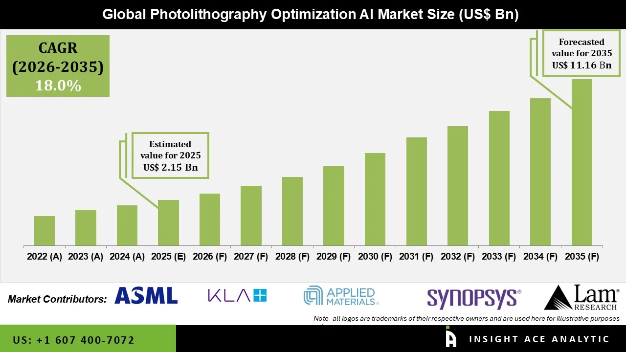
Photolithography optimization AI implies an application of artificial intelligence solutions for enhancing the efficiency and precision of semiconductor fabrication processes involving photolithography techniques. Algorithms based on AI technology use huge volumes of manufacturing data to optimize process exposure parameters, detect process deviations and defects, forecast system failures, and increase yields. Solutions based on AI become very important nowadays, considering that semiconductor makers switch to 5nm, 3nm, and other advanced process nodes.
The increasing need for powerful processors designed for AI, cloud computing, automobiles electronics, gadgets, and other applications stimulates investments into new semiconductor fabrication technologies. With more advanced and complicated chip designs appearing, it becomes impossible to apply conventional optimization solutions. AI photolithography optimization solutions help increase manufacturing efficiency and reduce process deviations.
Investments in fabrication units for semiconductors being made in countries like United States, Europe, China, South Korea, Taiwan, Japan, and India will drive the market forward. Government policies promoting semiconductor manufacturing domestically have spurred intelligent manufacturing technologies such as AI-enabled software for lithography optimizations. AI is being combined with computational lithography, digital twins, advanced metrology solutions, and process control solutions to boost product quality as well as reduce production cost.
Additionally, the shift towards the EUV lithography technique has increased the level of complexity in manufacturing process. The help of AI can be sought from manufacturers for the optimization of exposure processes, defect detection, overlay optimization, and preventive maintenance scheduling for equipment. The integration of AI with automation of factories, robotics, and smart manufacturing will contribute towards the market's growth in the forecast period.
Competitive Landscape
Which are the Leading Players in Photolithography Optimization AI Market?
• ASML Holding N.V.
• KLA Corporation
• Applied Materials Inc.
• Lam Research Corporation
• Tokyo Electron Limited (TEL)
• Synopsys Inc.
• Siemens EDA
• Cadence Design Systems
• NVIDIA Corporation
• IBM Corporation
• TSMC
• Samsung Electronics
• Intel Corporation
• Canon Inc.
• Nikon Corporation
• Onto Innovation
• Hitachi High-Tech Corporation
• Advantest Corporation
• Keysight Technologies
• PDF Solutions Inc.
• Siemens Digital Industries Software
• Cohu Inc.
• SCREEN Semiconductor Solutions
• Teradyne Inc.
• imec
• GLOBALFOUNDRIES
• Tower Semiconductor
• Renesas Electronics
• Qualcomm Technologies
• MediaTek Inc.
Market Dynamics
Driver
Rising Adoption of AI for Advanced Semiconductor Manufacturing
The increasing complexity of the fabrication process in semiconductors is among the most significant reasons behind the growth of the photolithography optimization artificial intelligence market. As manufacturers keep developing smaller nodes for transistors, the ability to have efficient production yield becomes more difficult. By optimizing the parameters of lithography through processing the relevant data from the process and detecting hidden variations in the process, AI prevents defects and, hence, saves on production. Furthermore, AI makes it possible to perform predictive maintenance of lithography machines and decrease unexpected downtime. With the rising trend of implementing smart factories as well as Industry 4.0 production process in semiconductors, the demand for such solutions is rapidly increasing.
Restrain/Challenge
High Implementation Cost and Limited Availability of Quality Manufacturing Data
While offering many benefits, the deployment of the AI-based photolithography optimization solution involves significant costs for the purchase of advanced computer hardware, powerful CPUs, software implementation, and specialized staff. Furthermore, a large amount of high-quality data is necessary for the training of artificial intelligence algorithms. Security concerns related to the data, discrepancies in the data sets created during production, and lack of access to sensitive information about the semiconductor processes hinder the implementation. This problem will hinder the deployment by smaller semiconductor producers.
Semiconductor Manufacturing Segment is Expected to Drive the Photolithography Optimization AI Market
It is anticipated that the semiconductor manufacturing segment will lead the market in terms of market share during the prediction period. It is a semiconductor manufacturing sector that produces chips for various clients through state-of-the-art process technology and focuses primarily on productivity and optimized yield. Artificial intelligence-based photolithography optimization facilitates process variance reduction, improved wafer uniformity, optimized exposure parameters, and low defect densities for high-volume manufacturing processes. With the rising need for AI processors, automotive ICs, advanced logic ICs, and high-performance computing ICs, foundries will be highly motivated to invest in intelligent lithography optimization software. Moreover, top-ranked foundries are relying on AI-powered process control systems combined with metrology and inspection tools to increase manufacturing accuracy while reducing the cost of production.
Machine Learning Segment is Growing at the Highest Rate in the Photolithography Optimization AI Market
Machine learning is anticipated to have the highest growth rate among all segments. Machine learning algorithms analyze millions of process data that occur in the manufacturing process of semiconductors, thus revealing patterns that traditional statistical methods cannot capture. This helps manufacturers in forecasting defects, optimizing exposure sequences, ensuring overlay accuracy and giving recommendations for corrective action even before problems happen during production. Moreover, machine learning allows predicting failures of lithography tools for preventive maintenance, thus decreasing downtime. Given that smart manufacturing and Industry 4.0 practices become increasingly common in the semiconductors manufacturing industry, the adoption of machine learning optimization solutions is set to rise sharply.
Why North America Led the Photolithography Optimization AI Market?
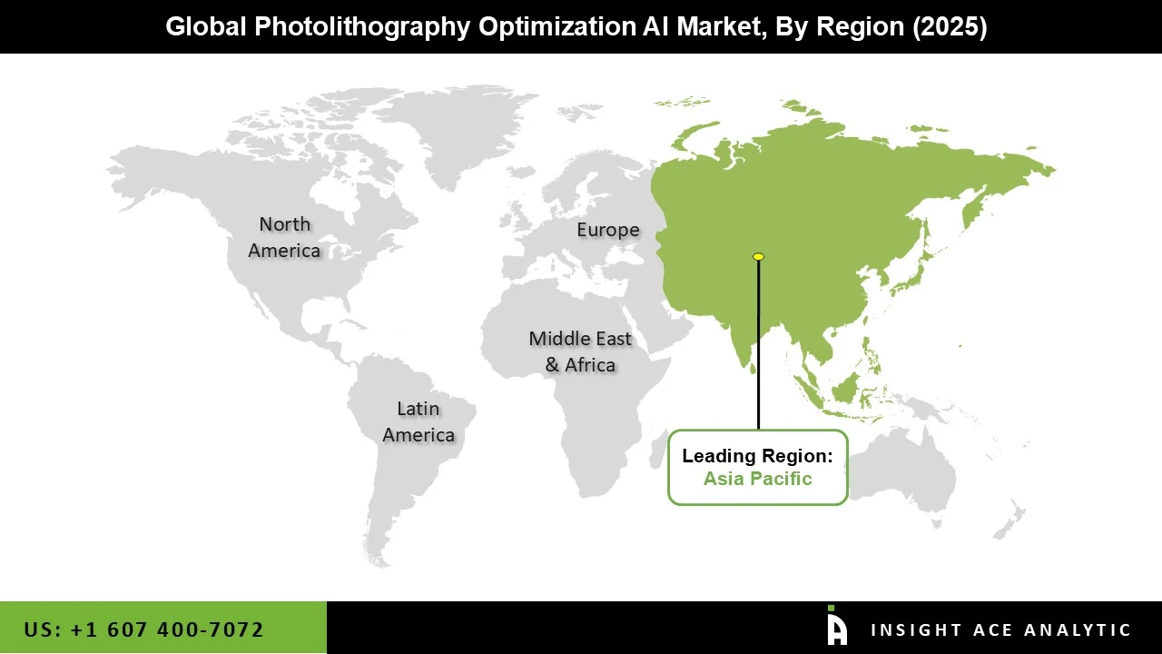
North America dominated the photolithography optimization AI market as a result of its well-established semiconductor manufacturing ecosystem, robust research capacities, and investment in AI technologies. Many semiconductor manufacturing equipment makers, as well as AI software makers, and IDMs in North America were constantly innovating intelligent manufacturing techniques. Programs launched to support the development of semiconductor manufacturing capabilities and rising investments in state-of-the-art facilities resulted in growing use of AI in different stages of semiconductor manufacturing process. Furthermore, cooperation between semiconductor firms, software firms, and research organizations further supported the developments in computational lithography, defects inspection, and yield optimization. Availability of firms that offer high-performance computing capacity has also facilitated the creation and application of sophisticated AI algorithms to process manufacturing data in real time.
Key Development:
June 2025: ASML Holding upgraded its AI-based computational lithography platform using process optimization software that enhances EUV pattern precision, variability in exposure, and wafer production process for advanced semiconductor nodes.
May 2025: KLA Corporation launched its new AI-based semiconductor defect inspection and process control solutions to detect pattern defects at nanoscale quickly and enhance yield from semiconductors by real-time analytics.
March 2025: Applied Materials launched the next generation of its AI-based semiconductor manufacturing platform through the integration of machine learning model in process control systems to improve the lithography process.
October 2024: Synopsys upgraded its computational lithography software platform with AI-based capabilities for accelerating mask optimization, improving optical proximity correction (OPC) process, and optimizing semiconductor design cycle.
September 2024: Siemens EDA upgraded its AI-based digital twin solution for semiconductor manufacturing processes for predictive process optimization and efficient lithography process management.
July 2024: Lam Research introduced advanced analytics using AI technologies for semiconductor fabrication equipment to improve production process and minimize downtimes in manufacturing.
Photolithography Optimization AI Market Report Scope:
| Report Attribute | Specifications |
| Market size value in 2025 | USD 2.15 Bn |
| Revenue forecast in 2035 | USD 11.16 Bn |
| Growth Rate CAGR | CAGR of 18.0% from 2026 to 2035 |
| Quantitative Units | Representation of revenue in US$ Bn and CAGR from 2026 to 2035 |
| Historic Year | 2022 to 2025 |
| Forecast Year | 2026-2035 |
| Report Coverage | The forecast of revenue, the position of the company, the competitive market structure, growth prospects, and trends |
| Segments Covered | Component, Technology, Application, Deployment Mode, End-user, and By Region |
| Regional Scope | North America; Europe; Asia Pacific; Latin America; Middle East & Africa |
| Country Scope | U.S.; Canada; U.K.; Germany; China; India; Japan; Brazil; Mexico; The UK; France; Italy; Spain; China; Japan; India; South Korea; Southeast Asia; South Korea; Southeast Asia |
| Competitive Landscape | ASML Holding N.V., KLA Corporation, Applied Materials Inc., Lam Research Corporation, Tokyo Electron Limited, Synopsys Inc., Siemens EDA, Cadence Design Systems, NVIDIA Corporation, IBM Corporation, TSMC, Samsung Electronics, Intel Corporation, Canon Inc., Nikon Corporation, Onto Innovation, PDF Solutions Inc., SCREEN Semiconductor Solutions, Hitachi High-Tech Corporation, and others. |
| Customization Scope | Free customization report with the procurement of the report, Modifications to the regional and segment scope. Geographic competitive landscape. |
| Pricing and Available Payment Methods | Explore pricing alternatives that are customized to your particular study requirements. |
Photolithography Optimization AI Market Segmentation:
Photolithography Optimization AI Market by Component -
• Software
• Hardware
• Services
Photolithography Optimization AI Market by Technology -
• Deep Learning
• Machine Learning
• Computer Vision
• Others
Photolithography Optimization AI Market by Application -
• Semiconductor Manufacturing
• MEMS Fabrication
• Advanced Packaging
• Others
Photolithography Optimization AI Market by Deployment Mode -
• On-Premises
• Cloud
Photolithography Optimization AI Market by End-user-
• IDMs
• Foundries
• Research Institutes
• Others
Photolithography Optimization AI Market- By Region-
North America-
• The US
• Canada
Europe-
• Germany
• The UK
• France
• Italy
• Spain
• Rest of Europe
Asia-Pacific-
• China
• Japan
• India
• South Korea
• South East Asia
• Rest of Asia Pacific
Latin America-
• Brazil
• Argentina
• Mexico
• Rest of Latin America
Middle East & Africa-
• GCC Countries
• South Africa
• Rest of Middle East and Africa
Research Design and Approach
This study employed a multi-step, mixed-method research approach that integrates:
- Secondary research
- Primary research
- Data triangulation
- Hybrid top-down and bottom-up modelling
- Forecasting and scenario analysis
This approach ensures a balanced and validated understanding of both macro- and micro-level market factors influencing the market.
Secondary Research
Secondary research for this study involved the collection, review, and analysis of publicly available and paid data sources to build the initial fact base, understand historical market behaviour, identify data gaps, and refine the hypotheses for primary research.
Sources Consulted
Secondary data for the market study was gathered from multiple credible sources, including:
- Government databases, regulatory bodies, and public institutions
- International organizations (WHO, OECD, IMF, World Bank, etc.)
- Commercial and paid databases
- Industry associations, trade publications, and technical journals
- Company annual reports, investor presentations, press releases, and SEC filings
- Academic research papers, patents, and scientific literature
- Previous market research publications and syndicated reports
These sources were used to compile historical data, market volumes/prices, industry trends, technological developments, and competitive insights.
Primary Research
Primary research was conducted to validate secondary data, understand real-time market dynamics, capture price points and adoption trends, and verify the assumptions used in the market modelling.
Stakeholders Interviewed
Primary interviews for this study involved:
- Manufacturers and suppliers in the market value chain
- Distributors, channel partners, and integrators
- End-users / customers (e.g., hospitals, labs, enterprises, consumers, etc., depending on the market)
- Industry experts, technology specialists, consultants, and regulatory professionals
- Senior executives (CEOs, CTOs, VPs, Directors) and product managers
Interview Process
Interviews were conducted via:
- Structured and semi-structured questionnaires
- Telephonic and video interactions
- Email correspondences
- Expert consultation sessions
Primary insights were incorporated into demand modelling, pricing analysis, technology evaluation, and market share estimation.
Data Processing, Normalization, and Validation
All collected data were processed and normalized to ensure consistency and comparability across regions and time frames.
The data validation process included:
- Standardization of units (currency conversions, volume units, inflation adjustments)
- Cross-verification of data points across multiple secondary sources
- Normalization of inconsistent datasets
- Identification and resolution of data gaps
- Outlier detection and removal through algorithmic and manual checks
- Plausibility and coherence checks across segments and geographies
This ensured that the dataset used for modelling was clean, robust, and reliable.
Market Size Estimation and Data Triangulation
Bottom-Up Approach
The bottom-up approach involved aggregating segment-level data, such as:
- Company revenues
- Product-level sales
- Installed base/usage volumes
- Adoption and penetration rates
- Pricing analysis
This method was primarily used when detailed micro-level market data were available.
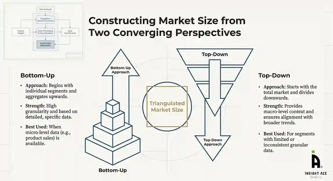
Top-Down Approach
The top-down approach used macro-level indicators:
- Parent market benchmarks
- Global/regional industry trends
- Economic indicators (GDP, demographics, spending patterns)
- Penetration and usage ratios
This approach was used for segments where granular data were limited or inconsistent.
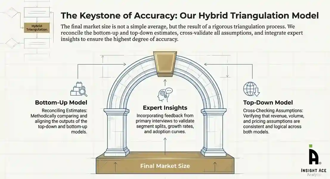
Hybrid Triangulation Approach
To ensure accuracy, a triangulated hybrid model was used. This included:
- Reconciling top-down and bottom-up estimates
- Cross-checking revenues, volumes, and pricing assumptions
- Incorporating expert insights to validate segment splits and adoption rates
This multi-angle validation yielded the final market size.
Forecasting Framework and Scenario Modelling
Market forecasts were developed using a combination of time-series modelling, adoption curve analysis, and driver-based forecasting tools.
Forecasting Methods
- Time-series modelling
- S-curve and diffusion models (for emerging technologies)
- Driver-based forecasting (GDP, disposable income, adoption rates, regulatory changes)
- Price elasticity models
- Market maturity and lifecycle-based projections
Scenario Analysis
Given inherent uncertainties, three scenarios were constructed:
- Base-Case Scenario: Expected trajectory under current conditions
- Optimistic Scenario: High adoption, favourable regulation, strong economic tailwinds
- Conservative Scenario: Slow adoption, regulatory delays, economic constraints
Sensitivity testing was conducted on key variables, including pricing, demand elasticity, and regional adoption.
Request Customization
Add countries, segments, company profiles, or extend forecast — free 10% customization with purchase.
Customize This Report →Enquire Before Buying
Speak with our analyst team about scope, methodology, pricing, or deliverable formats.
Enquire Now →Frequently Asked Questions
Photolithography Optimization AI Market Size is valued at USD 2.15 Bn in 2025 and is predicted to reach USD 11.16 Bn by the year 2035
Next Generation Data Storage Market is expected to grow at a 18.0% CAGR during the forecast period for 2026 to 2035.
ASML Holding N.V., KLA Corporation, Applied Materials Inc., Lam Research Corporation, Tokyo Electron Limited, Synopsys Inc., Siemens EDA, Cadence Design Systems, NVIDIA Corporation, IBM Corporation, TSMC, Samsung Electronics, Intel Corporation, Canon Inc., Nikon Corporation, Onto Innovation, PDF Solutions Inc., SCREEN Semiconductor Solutions, Hitachi High-Tech Corporation, and others.
Photolithography Optimization AI Market is segmented into Component, Technology, Application, Deployment Mode, End-user, and By Region
North America region is leading the Photolithography Optimization AI Market.