EUV Mask Inspection Systems Market Size, Share, Trend, Forecast Report 2026 to 2035
What is EUV Mask Inspection Systems Market Size?
EUV Mask Inspection Systems Market Size is valued at USD 1.86 Bn in 2025 and is predicted to reach USD 5.98 Bn by the year 2035 at a 12.5% CAGR during the forecast period for 2026 to 2035.
EUV Mask Inspection Systems Market Size, Share & Trends Analysis by Type (Die-to-Die Inspection, Die-to-Database Inspection), by Technology (Optical, E-Beam, Others), by Application (Semiconductor Manufacturing, Integrated Circuits, MEMS, Others), by End-User (Foundries, IDMs, OSATs, Others), and Segment Forecasts, 2026 to 2035
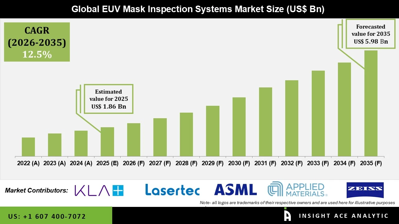
The market for EUV mask inspection systems is becoming quite prominent for semiconductor manufacturers who are shifting towards more advanced semiconductor processing nodes lower than 5 nm. The extreme ultraviolet (EUV) lithography technology helps produce highly complex semiconductors, where even the presence of a small defect in an EUV mask would lead to a decrease in a manufacturing yield. Therefore, the development of the inspection systems for detecting nanometer-scale defects became vital for semiconductor manufacturing process.
Increasing investments in semiconductor fabrication facilities, growing needs for processors for artificial intelligence, HPC systems, automobiles, and memory devices are making the semiconductor companies use EUV mask inspection systems globally. There are constant efforts to improve manufacturing yields while decreasing cost-effectiveness, which leads to the increasing need for advanced inspection technologies.
Moving forward toward the 3 nm, 2 nm, and the other future semiconductor nodes is making a demand for the actinic inspection technologies, which will help to detect defects by real EUV wavelengths. Moreover, government policies on developing domestic semiconductor manufacturing in the US, Europe, Japan, South Korea, Taiwan, and India are providing new opportunities for the vendors of the inspection technologies.
Despite numerous advantages, the segment experiences several barriers to its development, such as extremely high prices of the inspection equipment, complicated system integration, and low number of suppliers of advanced EUV mask inspection systems. Nonetheless, there are constant technological improvements in high-resolution optics, artificial intelligence defect detection, multi-beam electron inspection, and automation that are supporting market growth.
Competitive Landscape
Which are the Leading Players in EUV Mask Inspection Systems Market?
• KLA Corporation
• Lasertec Corporation
• ASML Holding N.V.
• Carl Zeiss SMT GmbH
• Applied Materials Inc.
• Hitachi High-Tech Corporation
• Hermes Microvision Inc. (ASML)
• NuFlare Technology Inc.
• Nikon Corporation
• Advantest Corporation
• Onto Innovation Inc.
• JEOL Ltd.
• SCREEN Semiconductor Solutions
• Toray Engineering Co., Ltd.
• Hamamatsu Photonics K.K.
• HOYA Corporation
• Toppan Photomasks Inc.
• Photronics Inc.
• DNP (Dai Nippon Printing Co., Ltd.)
• Intel Corporation (R&D collaborations)
Market Dynamics
Driver
Growing Adoption of EUV Lithography in Advanced Semiconductor Manufacturing
The speedy adoption of the EUV lithography process for the manufacturing of semiconductor products is one of the biggest factors behind the growth in EUV mask inspection system market. Manufacturers are continuously investing in EUV lithography to produce processors that could be used in artificial intelligence, cloud computing, data centers, self-driving cars, consumer devices, and communication infrastructure. With the continuous reduction in the size of semiconductors, traditional optical inspection systems find it difficult to detect small defects. Advanced EUV mask inspection systems help manufacturers identify small defects with greater sensitivity and improve yield. Growing investments in the establishment of new fabrication facilities for semiconductors in countries in Asia-Pacific region, North America, and Europe and growing government support through semiconductor incentive programs are driving the market for mask inspection systems even further. Furthermore, the increasing use of artificial intelligence in inspecting defects is another factor driving the demand.
Restrain/Challenge
High Capital Investment and Limited Availability of Advanced Inspection Technologies
Some of the main concerns which hinder the development of EUV mask inspection systems market include the very expensive process involved in the development and deployment of new technology. EUV inspection tools require optical elements and ultra-high vacuum system together with sophisticated stages and detectors, thus, the cost is considerable. Furthermore, only a few manufacturers have technological capability to provide the necessary actinic EUV inspection tool, and hence this poses limitations on the entire semiconductor industry. Product development is not an easy task since it takes long time, coupled with increased costs of maintenance and also lack of skilled technical personnel. There are technological advancements which are needed to be implemented to meet up the ever-changing semiconductor designs.
Foundries Segment is Expected to Drive the EUV Mask Inspection Systems Market
The foundries segment is estimated to capture the maximum market share for the EUV mask inspection systems market over the projected time frame. Major foundry players are rapidly augmenting their EUV lithography manufacturing capacity to produce advanced chips for AI, HPC, 5G technology, automotive electronics, and data centers. With even minute mask defects potentially impacting the quality of wafers, major investments are being made in advanced inspection systems with high-resolution capabilities to detect any potential defects prior to manufacturing operations. Increasing spending on new generation fabs, increasing production capacity, and advancements in 3 nm and 2 nm process technologies are anticipated to bolster market growth opportunities from semiconductor foundries over the upcoming period. Besides, AI-powered defect analysis software is increasingly becoming a norm among major manufacturers.
Die-to-Database (D2DB) Inspection Segment is Growing at the Highest Rate in the EUV Mask Inspection Systems Market
Die-to-Database (D2DB) inspection dominates because it compares the actual mask pattern directly against the original design database, providing a highly reliable reference for identifying pattern defects, missing or extra features, dimensional deviations, and other mask-writing errors. Unlike die-to-die inspection, D2DB does not require two identical dies on the mask, making it particularly valuable for single-die, complex, and advanced-node EUV masks. KLA’s commercial reticle inspection platforms support both die-to-database and die-to-die inspection, highlighting D2DB’s established importance in advanced mask manufacturing.
Its importance increases with EUV because extremely small pattern defects can affect wafer printing and manufacturing yield. D2DB enables comprehensive pattern verification against intended design data and supports sophisticated computational modeling to improve inspection sensitivity. Growing mask complexity, tighter process tolerances, and the transition toward advanced EUV nodes therefore support the segment’s dominant market position.
Why Asia-Pacific Led the EUV Mask Inspection Systems Market?
Asia-Pacific is predicted to account for a large proportion of the global EUV mask inspection systems market throughout the forecast period. Favorable investments in research in semiconductors and semiconductor manufacturing processes along with government efforts to enhance the domestic manufacturing capabilities for the semiconductor products is a major contributing factor in driving the development of innovative mask inspection systems. Investments in the field of AI processors, military electronics, cloud computing, and next-generation semiconductor manufacturing operations are fueling the demand for advanced inspection systems for masks.
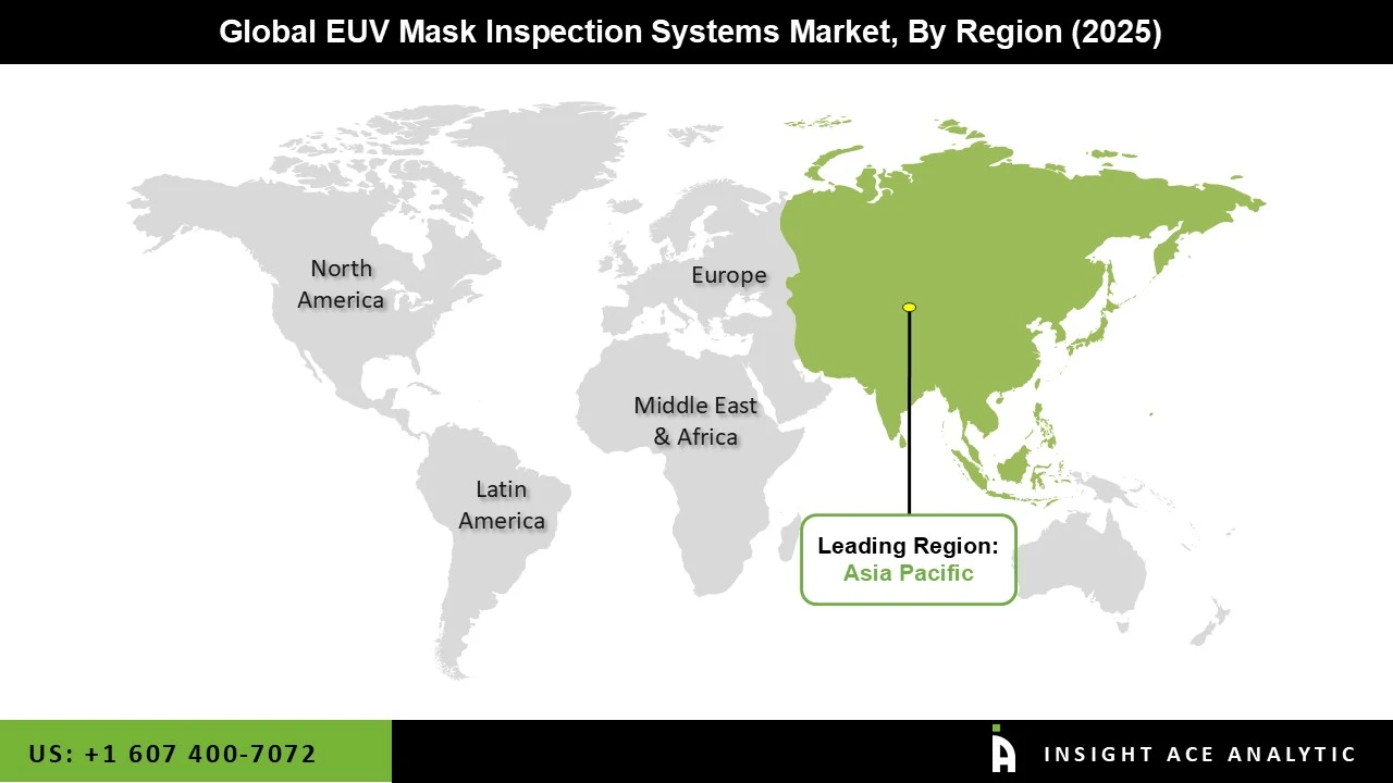
The Asia-Pacific is predicted to experience a relatively fast growth rate for the market throughout the forecast period. Emerging semiconductor manufacturing facilities in several countries in the Asia-Pacific such as Taiwan, South Korea, Japan, China, and India with significant investments in the advanced manufacturing facilities is contributing significantly towards the growth of this market. Moreover, increasing demand for consumer electronics, electric vehicle components, high-performance computing chips, and artificial intelligence accelerators is prompting manufacturers to implement advanced inspection machines.
Key Development:
June 2025: KLA Corporation added to its advanced reticle inspection offerings by providing AI-driven defect inspection tools with improved defect classification capabilities that are meant to be used for EUV semiconductor manufacturing.
April 2025: Lasertec Corporation upgraded their actinic mask inspection offering to provide better sensitivity to detect ultra-fine printable defects needed for semiconductor production.
February 2025: ASML Holding N.V. made further investments in High-NA EUV ecosystem through partnerships with semiconductor makers and suppliers in order to optimize mask inspection process for future technology node manufacturing.
September 2024: Hitachi High-Tech Corporation offered new high resolution e-beam inspection technologies intended to increase defect inspection for semiconductors and cut down inspection time.
May 2024: Applied Materials Inc. extended their process control for semiconductors line with advanced innovations in inspection and metrology fields.
EUV Mask Inspection Systems Market Report Scope:
| Report Attribute | Specifications |
| Market size value in 2025 | USD 1.86 Bn |
| Revenue forecast in 2035 | USD 5.98 Bn |
| Growth Rate CAGR | CAGR of 12.5% from 2026 to 2035 |
| Quantitative Units | Representation of revenue in US$ Bn and CAGR from 2026 to 2035 |
| Historic Year | 2022 to 2025 |
| Forecast Year | 2026-2035 |
| Report Coverage | The forecast of revenue, the position of the company, the competitive market structure, growth prospects, and trends |
| Segments Covered | Type, Technology, Application, End-user, and By Region |
| Regional Scope | North America; Europe; Asia Pacific; Latin America; Middle East & Africa |
| Country Scope | U.S.; Canada; U.K.; Germany; China; India; Japan; Brazil; Mexico; The UK; France; Italy; Spain; China; Japan; India; South Korea; Southeast Asia; South Korea; Southeast Asia |
| Competitive Landscape | KLA Corporation, Lasertec Corporation, ASML Holding N.V., Carl Zeiss SMT GmbH, Applied Materials Inc., Hitachi High-Tech Corporation, Hermes Microvision Inc. (ASML), NuFlare Technology Inc., Nikon Corporation, Advantest Corporation, Onto Innovation Inc., JEOL Ltd., SCREEN Semiconductor Solutions, Toray Engineering Co., Ltd., Hamamatsu Photonics K.K., HOYA Corporation, Toppan Photomasks Inc., Photronics Inc., DNP (Dai Nippon Printing Co., Ltd.), and Intel Corporation (R&D collaborations). |
| Customization Scope | Free customization report with the procurement of the report, Modifications to the regional and segment scope. Geographic competitive landscape. |
| Pricing and Available Payment Methods | Explore pricing alternatives that are customized to your particular study requirements. |
EUV Mask Inspection Systems Market Segmentation:
EUV Mask Inspection Systems Market by Type-
• Die-to-Die Inspection
• Die-to-Database Inspection
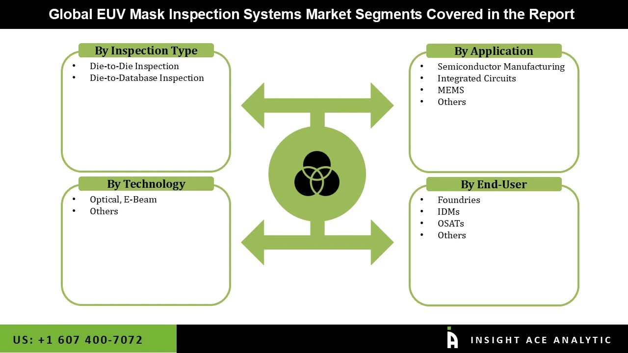
EUV Mask Inspection Systems Market by Technology -
• Optical
• E-Beam
• Others
EUV Mask Inspection Systems Market by Application-
• Semiconductor Manufacturing
• Integrated Circuits
• MEMS
• Others
EUV Mask Inspection Systems Market by End-user -
• Foundries
• IDMs
• OSATs
• Others
EUV Mask Inspection Systems Market-By Region-
North America-
• The US
• Canada
Europe-
• Germany
• The UK
• France
• Italy
• Spain
• Rest of Europe
Asia-Pacific-
• China
• Japan
• India
• South Korea
• South East Asia
• Rest of Asia Pacific
Latin America-
• Brazil
• Argentina
• Mexico
• Rest of Latin America
Middle East & Africa-
• GCC Countries
• South Africa
• Rest of Middle East and Africa
Research Design and Approach
This study employed a multi-step, mixed-method research approach that integrates:
- Secondary research
- Primary research
- Data triangulation
- Hybrid top-down and bottom-up modelling
- Forecasting and scenario analysis
This approach ensures a balanced and validated understanding of both macro- and micro-level market factors influencing the market.
Secondary Research
Secondary research for this study involved the collection, review, and analysis of publicly available and paid data sources to build the initial fact base, understand historical market behaviour, identify data gaps, and refine the hypotheses for primary research.
Sources Consulted
Secondary data for the market study was gathered from multiple credible sources, including:
- Government databases, regulatory bodies, and public institutions
- International organizations (WHO, OECD, IMF, World Bank, etc.)
- Commercial and paid databases
- Industry associations, trade publications, and technical journals
- Company annual reports, investor presentations, press releases, and SEC filings
- Academic research papers, patents, and scientific literature
- Previous market research publications and syndicated reports
These sources were used to compile historical data, market volumes/prices, industry trends, technological developments, and competitive insights.
Primary Research
Primary research was conducted to validate secondary data, understand real-time market dynamics, capture price points and adoption trends, and verify the assumptions used in the market modelling.
Stakeholders Interviewed
Primary interviews for this study involved:
- Manufacturers and suppliers in the market value chain
- Distributors, channel partners, and integrators
- End-users / customers (e.g., hospitals, labs, enterprises, consumers, etc., depending on the market)
- Industry experts, technology specialists, consultants, and regulatory professionals
- Senior executives (CEOs, CTOs, VPs, Directors) and product managers
Interview Process
Interviews were conducted via:
- Structured and semi-structured questionnaires
- Telephonic and video interactions
- Email correspondences
- Expert consultation sessions
Primary insights were incorporated into demand modelling, pricing analysis, technology evaluation, and market share estimation.
Data Processing, Normalization, and Validation
All collected data were processed and normalized to ensure consistency and comparability across regions and time frames.
The data validation process included:
- Standardization of units (currency conversions, volume units, inflation adjustments)
- Cross-verification of data points across multiple secondary sources
- Normalization of inconsistent datasets
- Identification and resolution of data gaps
- Outlier detection and removal through algorithmic and manual checks
- Plausibility and coherence checks across segments and geographies
This ensured that the dataset used for modelling was clean, robust, and reliable.
Market Size Estimation and Data Triangulation
Bottom-Up Approach
The bottom-up approach involved aggregating segment-level data, such as:
- Company revenues
- Product-level sales
- Installed base/usage volumes
- Adoption and penetration rates
- Pricing analysis
This method was primarily used when detailed micro-level market data were available.

Top-Down Approach
The top-down approach used macro-level indicators:
- Parent market benchmarks
- Global/regional industry trends
- Economic indicators (GDP, demographics, spending patterns)
- Penetration and usage ratios
This approach was used for segments where granular data were limited or inconsistent.
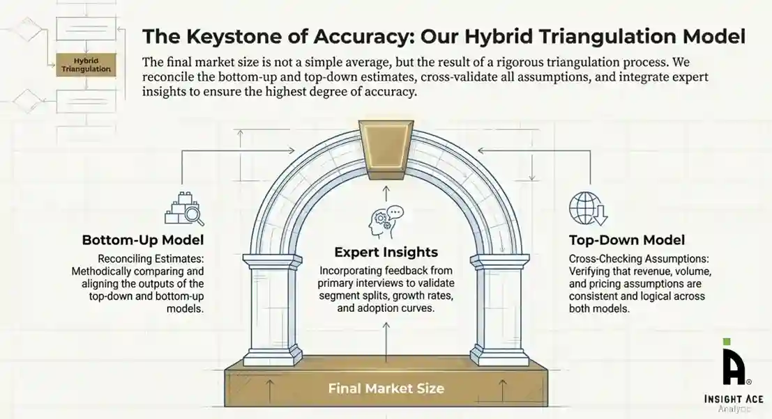
Hybrid Triangulation Approach
To ensure accuracy, a triangulated hybrid model was used. This included:
- Reconciling top-down and bottom-up estimates
- Cross-checking revenues, volumes, and pricing assumptions
- Incorporating expert insights to validate segment splits and adoption rates
This multi-angle validation yielded the final market size.
Forecasting Framework and Scenario Modelling
Market forecasts were developed using a combination of time-series modelling, adoption curve analysis, and driver-based forecasting tools.
Forecasting Methods
- Time-series modelling
- S-curve and diffusion models (for emerging technologies)
- Driver-based forecasting (GDP, disposable income, adoption rates, regulatory changes)
- Price elasticity models
- Market maturity and lifecycle-based projections
Scenario Analysis
Given inherent uncertainties, three scenarios were constructed:
- Base-Case Scenario: Expected trajectory under current conditions
- Optimistic Scenario: High adoption, favourable regulation, strong economic tailwinds
- Conservative Scenario: Slow adoption, regulatory delays, economic constraints
Sensitivity testing was conducted on key variables, including pricing, demand elasticity, and regional adoption.
Request Customization
Add countries, segments, company profiles, or extend forecast — free 10% customization with purchase.
Customize This Report →Enquire Before Buying
Speak with our analyst team about scope, methodology, pricing, or deliverable formats.
Enquire Now →Frequently Asked Questions
EUV Mask Inspection Systems Market Size is valued at USD 1.86 Bn in 2025 and is predicted to reach USD 5.98 Bn by the year 2035
EUV Mask Inspection Systems Market is expected to grow at a 12.5% CAGR during the forecast period for 2026 to 2035.
KLA Corporation, Lasertec Corporation, ASML Holding N.V., Carl Zeiss SMT GmbH, Applied Materials Inc., Hitachi High-Tech Corporation, Hermes Microvision Inc. (ASML), NuFlare Technology Inc., Nikon Corporation, Advantest Corporation, Onto Innovation Inc., JEOL Ltd., SCREEN Semiconductor Solutions, Toray Engineering Co., Ltd., Hamamatsu Photonics K.K., HOYA Corporation, Toppan Photomasks Inc., Photronics Inc., DNP (Dai Nippon Printing Co., Ltd.), and Intel Corporation (R&D collaborations).
EUV Mask Inspection Systems Market is segmented into Type, Technology, Application, End-user, and By Region
Asia Pacific region is leading the EUV Mask Inspection Systems Market.